Page 120 - Maxwell House
P. 120
100                                                                Chapter 2


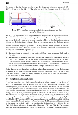
          assuming that the electron  mobility is µ = 50, the average relaxation time   = 0.135 ∙
         0
        10 −12   [s], and  0 ≤  0  ≤ 1  [T]. The  solid  red and blue  lines correspond to  | ⁄  |

                                                                                  0


                Figure 2.9.7 Normalized graphene conductivity versus frequency and  :
                                                                         0
                                     a)  ⁄ , b)  ⁄  0


                                            0

        and | ⁄  |, respectively, while the green indicates the phase shift in degrees between them.

                 0
        The plots demonstrate the way how to use graphene in tunable, i.e. reconfigurable, microwave
        and optical devices by varying the external magnetic field. Since the electron is enormously
        light particle the tuning time is extremely short, as it is required in ultra-fast electronic devices.
        Another interesting  magnetic  phenomenon in  magnetically biased graphene  is so-called
        Faraday magneto-optical effect that causes a linear polarized EM wave to change or rotate its
        polarization.  Such effect is explained by
        1.  The dependence  of conductivity current  from E-field vector  orientation (look back at
            (2.104)).
        2.  The existence of  non-zero  phase  shift  between  the conductivity components  shown in
            Figure 2.9.7b. As such, each of two orthogonal component of E-field gets its “personal”
            phase shift while passing graphene layer in the direction of  . Correspondingly, the total
                                                            0
            E-field vector of propagation wave changes its orientation, i.e. rotates. We will demonstrate
            this effect in section 6.7 of Chapter 6 on the example of magnetized ferrite.
        By far, the vast variety of graphene-based non-reciprocal microwave and optical devices based
        on Faraday effect is developed. They include isolators, circulators, gyrators, phase shifters,
        polarizers, switches, tunable  resonators, and tunable filters. All of them are  ubiquitous in
        modern telecommunication systems.

        2.9.4   Graphene as Shielding Material
        It was hard to believe, but a single sheet of graphene of only one atom thick can detect and
        absorb EM radiation having a wavelength much higher than its dimensions. It becomes more
        understandable if we recall that such graphene layer possesses large number of free electrons
                      2
        (~3.8∙ 10 per m ) located on each side of layer lattice. The experiments demonstrate that one-
                17
        layer undoped graphene sheet provides a relatively mild reduction in passing through EM wave
        energy, around 2.27  dB, which  corresponds to  a  loss  of 41% of carried by fields’ energy.
        Nevertheless, the five-layer sandwich structure is able, at last in theory, to absorb almost 70%
        of  passing  EM energy. Assuming that the  monolayer  graphene  is printed  on polyethylene
        terephthalate (PET) substrate of 0.01 mm thickness the expected total thickness of this shielding
        screen is around 0.05mm + negligible 1.7nm of graphene (!). The experimental data published
        to date let suggest the high feasibility of manufacturing the broadband, ultra thin and flexible
        EMI shield  in the  microwave frequency band between  1  GHz and 26 GHz. The graphene
        shielding promises remarkable extra benefits. Because the graphene conductivity depends on

