Page 117 - Maxwell House
P. 117
NEOCLASSICAL THEORY OF INTERACTION                                       97

            In section 2.2.6 of this chapter, we shortly discuss the drift of electrons inside the conductive
            medium under the influence of external E-field. When E-field is not strong enough to cause the
            nonlinear effects, the average electron drift velocity according to (2.28) is proportional to E-
            field strength and can be written as  = , where the parameter   is called the electron
                                                                    26

                                               2
            mobility and measured in [(m/s)/(V/m) = m /(V∙s)]. It was found that the electrons travel along
            graphene sheet extremely fast, about 20 kilometers (!) per second while the applied E-field
                                                         intensity is 10 V/m only (µ = 2000 [m /
                                                                                      2
                                                         (V·s)]  at room temperature  and
                                                         increases   to  10000  at  low
                                                         temperature). If so, it takes only 43 ns
                                                         for average electron pass the distance
                                                         1 mm that opens way for ultra-fast and
                                                         ultra-broadband connections  between
                                                         circuit elements and thereby ultra-fast
                       Microwave Band                    computer chips and transistors.  For
                                                         comparison, in average   =  13.5 in
             Figure 2.9.2 Graphene complex conductivity over   silicon,  = 39 in germanium,  = 60
                             frequency                   in GaAs,   =100 in InP,   =  95 in
                                                         silver, the best  metal conductor,  =
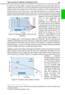
            57.7 in copper, and  = 26 in aluminum. Figure 2.9.2 illustrates  the real (solid lines) and
                                                                 27
            imaginary (dotted lines) part of the conductivity of single-layer graphene over the frequency at
            room temperature. The Fermi energy   [eV] has been selected as a parameter. Recall that

            the Fermi energy is a concept in quantum mechanics usually referring to the energy difference
            between the highest and lowest occupied single-particle states.
            Applying a positive gate voltage to the graphene will shift the Fermi level into the conduction
            band. A negative gate voltage will lower the Fermi level making holes the dominant carriers.
            Thereby, the gate, aka bias, voltage allows the dynamic control of both real and imaginary part
            of the conductivity According to Figure 2.9.2, graphene in the microwave range behaves like a
                                                                 moderate      conductor.
                                                                 Though graphene is the best
                                                                 electrical conductor known,
                                            =0.15 eV             it is mono-atomic and thus
                                                                 the surface resistance  =
                                                                                    □
                                                                 1/ ∙   is  relatively  high
                                                                 compared to metals at micro
                                                                 and mm-waves frequencies
                                                                 (see Figure 2.9.2),  even
                                                                 with the possibility of
                                                                 doping and electric field
                                                                 biasing. Nevertheless, it
                                                                 preserves the outstanding
                                                                 property of tunability.
                  Figure 2.9.3 Graphene relative dielectric constant


            26  Do not mix up this parameter with material permittivity. Such notification is customary in physics and
            we decided to keep it.
            27  All plots are derived using Kubo formula.

