
Page 308 - Maxwell House
P. 308
288 Chapter 6
more) while its thickness is about twice the gap width. Since the carrying energy is divided
between two gaps the Ohmic loss is lower and power handling is higher than in conventional
slotline.
q) A Grounded CPW (GCPW) is used on PCB as an alternative to microstrip line and behaves
mainly like microstrip. Due to vias connecting the ground planes, GCPW less radiates and
provides better isolation between adjacent lines than conventional microstrip. As a result, the
denser PCB can be fabricated. Since the biggest share of EM energy concentrates in dielectric,
GCPW is a low dispersive line. The Ohmic loss and power handling are similar to CPW.
r) and s) The first images illustrate how the fence of vias providing the Vertical Interconnect
Access (VIA) helps minimize the crosstalk between adjacent lines and support the signal trace
printed on a substrate of suspended stripline (see Figure 6.2.2d). Each via is a short metal rod
or the hole that passes through the dielectric substrate and metal ground planes is metallized on
the inside and provides the electric contact between the ground planes. In the case of the
microstrip line, the individual metal pads next to trace are printed on the top of the substrate as
shown in Figure 6.2.2s. In fact, it converts the microstrip line into GCPW. The rule of thumb
recommends that the spacing between two adjacent vias in fence must be as minimum one-
eighth of a wavelength in the dielectric. They also should be placed outside the field diameter
defined earlier not to disturb an EM wave propagation in line. In multi-layer PCB, the vias are
not only shielded the signal line traces but provide the electrical connections between layers.
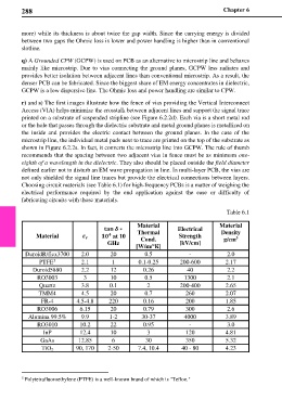
Choosing circuit materials (see Table 6.1) for high-frequency PCBs is a matter of weighing the
electrical performance required by the end application against the ease or difficulty of
fabricating circuits with those materials.
Table 6.1
Material Material
∗ Thermal Electrical Density
Material at 10 Cond. Strength g/cm
3
GHz [W/m/°] [kV/cm]
DuroidR/flex3700 2.0 20 0.5 - 2.0
5
PTFE 2.1 1 0.1-0.25 200-600 2.17
Duroid5880 2.2 12 0.26 40 2.2
RO3003 3 10 0.5 1300 2.1
Quartz 3.8 0.1 2 200-400 2.65
TMM4 4.5 20 0.7 260 2.07
FR-4 4.5-4.8 220 0.16 200 1.85
RO3006 6.15 20 0.79 300 2.6
Alumina 99.5% 9.9 1-2 30-37 4000 3.89
RO3010 10.2 22 0.95 - 3.0
InP 12.4 10 3 120 4.81
GaAs 12.85 6 30 350 5.32
TiO2 90, 170 2-50 7.4, 10.4 40 - 80 4.23
5 Polytetrafluoroethylene (PTFE) is a well-known brand of which is "Teflon."