
Page 304 - Maxwell House
P. 304
284 Chapter 6
e) A two-wire balanced line above the highly conductive surface. Such line is practically
equivalent to the simple two-wire line when the poles of RF source is connected between
wires only. It becomes a one-wire line if the one source pole is attached to the conductive
surface, i.e. grounded, while the second one is attached to only one of the wire or both of
them in parallel. The only one wire attachment has broad practical application letting
design the devices called directional couplers. EM fields surrounding the source wire
induce the electric current flow into the adjacent one-wire line thereby transferring the
portion of its EM energy there. We will discuss this effect of mutual coupling later.
f) An overhead three-wire and three-phase power line. It would not be an exaggeration to
call such lines the blood vessels of our civilization. They transfer enormous electrical
energy along great distances and then distribute it to many consumers.
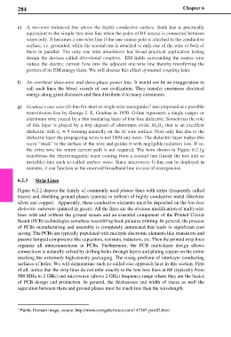
g) Goubau’s one-wire (G-line for short or single wire waveguide) was proposed as a possible
3
transmission line by George J. E. Goubau in 1950. G-line represents a single copper or
aluminum wire coated by a thin insulating layer of low loss dielectric. Sometimes the role
of this layer is played by a tiny deposit of aluminum oxide Al O that is an excellent
2 3
dielectric with ≅ 9 forming naturally on the Al wire surface. Note only that due to the
dielectric layer the propagating wave is not TEM any more. The dielectric layer makes this
wave “steak” to the surface of the wire and guides it with negligible radiation loss. If so,
the extra wire for return current path is not required. The horn shown in Figure 6.2.1g
transforms the electromagnetic wave coming from a coaxial line (inside the box and so
invisible) into such so-called surface wave. Since microwave G-line can be deployed in
minutes, it can function as the reserved broadband line in case of emergencies.
6.2.3 Strip Lines
Figure 6.2.2 depicts the family of commonly used planar lines with strips (frequently called
traces) and shielding ground planes (painted in yellow) of highly conductive metal (likewise
silver and copper). Apparently, these conductive elements must be deposited on the low-loss
dielectric substrate (painted in green). All the lines are the obvious modification of multi-wire
lines with and without the ground screen and an essential component of the Printed Circuit
Board (PCB) technologies somehow resembling book pictures printing. In general, the process
of PCBs manufacturing and assembly is completely automated that leads to significant cost
saving. The PCBs are typically populated with multiple electronic elements like transistors and
passive lumped components like capacitors, resistors, inductors, etc. Then the printed strip lines
organize all interconnections in PCBs. Furthermore, the PCB multi-layer design allows
connections is naturally solved by drilling holes through layers and plating copper on the entire
reaching the extremely high-density packaging. The rising problem of interlayer conducting
surfaces of holes. We will demonstrate such so-called vias approach later in this section. First
of all, notice that the strip lines do not refer exactly to the low-loss lines at RF (typically from
500 MHz to 2 GHz) and microwave (above 2 GHz) frequency range where they are the basics
of PCB design and production. In general, the thicknesses and width of traces as well the
separation between them and ground planes must be much less than the wavelength.
3 Public Domain image, source: http://www.energeticforum.com/147267-post82.html