
Page 315 - Maxwell House
P. 315
FEED LINE BASICS 295
cheese” longitudinal holes (white) of diameter ≪ and period ≪ . The main idea behind
the artificially produced photonic crystals, called Photonic Band Gap (PBG) crystals, is to alter
their structure in such manner that the light might pass freely through the crystal or be stopped
and reflected back at certain frequency ranges defined by crystal structure. From an engineering
point of view this structure are not more than 1D optical interference filters we will consider
later in Section 8.4.12 of Chapter 8. According to Figure 8.4.16a, the operation principle of 1D
periodic structure is based on the interference of multiple passing and reflected EM waves. As
we know, the acquired phase shift of EM waves is
defined by their frequency dependable propagation
coefficient k. As soon as all or most of the passing waves
get together in phase at some frequencies we have the
filter bandwidth while the in-phase grouping of reflected
waves means that the filter reflects at that frequencies
having bandstop. The material surrounding the central
hole and periodic PBG structure are developed in such
manner that it is equivalent to a bandstop filter
preventing the “lion’s share” of EM energy from
Figure 6.3.6 Illustration of propagating there. The result is a cable that in the lab was
PBG core with hole able to move data, using frequency-division
9
multiplexing , at a rate of 73.7 terabits per second, which
is approximately 1000 times better than standard fiber cable. Additional advantage of hollow-
core fiber is ability to withstand the loss increase due to fiber bending that is especially critical
for cable installation in the buildings. When a fiber cable is bent excessively, the optical signal
may escape from core through the fiber cladding and disappear. The standard bend radius
requirement is that it should exceed generally 20 - 25mm. The test of single hollow-core fiber
demonstrates that the bend of 5 mm radius adds 0.1 dB loss only.
6.3.4 Optical Waveguides
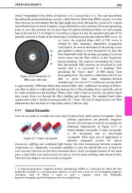
Now we are ready to consider one more type of optical feed called optical waveguides. Their
primary applications are photonic integrated
circuits. Several types of optical waveguides are
displayed schematically in Figure 6.3.7: a)
buried channel waveguide, b) ridge waveguide,
c) rib waveguide, and d) strip-loaded
Figure 6.3.7 Optic waveguide waveguide. Their main area of applications is
photonic integrated circuits for optical
processors, splitting and combining light beams, fast data transmission between computer
components, etc. Apparently, waveguide capability to carry the optical EM wave is based on
total internal reflection we just have discussed above. Each waveguide consists of two main
parts: a high-index core shown in red and one or two low-index cladding stabs shown in blue.
Note that core shape is not necessarily rectangular.
9 In telecommunications, frequency-division multiplexing (FDM) is a technique by which the total
bandwidth available in a communication medium is divided into a series of non-overlapping frequency
sub-bands, each of which is used to carry a separate signal (see Wikipedia,
https://en.wikipedia.org/wiki/Frequency-division_multiplexing)