Page 465 - Wago_AutomationTechnology_Volume3_2015_US.pdf
P. 465

6

                                                                                                                    463


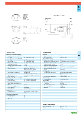
                     System bus    1: RD+/TD+
                   Input              Output  2: RD--/TD--                      Block diagram of an output
                                   3: TD--/RD--
                    4       4
                   1  5  3  3  5  1  4: TD+/RD+                     Digital Output                     Supply
                    2       2      5: GND
                                   Housing: Shield                  X1 ... X4
                        M12 B coded
                                                                    M12                                 M12
                                                                     1                                    2
                                                                     3                                    4
                  Digital Outputs X1 ... X4  1: 24 V U
                  (two outputs/connector)  3: 0 V U  A
                                        A
                   1  2     2  3             —  +  —  +                                        Logic  10 nF  10 nF
                   4  3     1  4                                     4/2
                                                                        270 pF
                        M12 A coded
                                   4: Output A
                                   2: Output B
                                                                                            Output  Error
                       Supply      1: 24 V U                                                0 ... 7  F  Module
                    Input               Output  2: 24 V U LS                                             mount
                                   3: 0 V U  A
                    2       2           LS
                   3  1    1  3    4: 0 V U A
                    4       4
                        M12 A coded


           Technical Data                                       Technical Data
           Information on actuator selection:                   Isolation:                                          6
            Delay time hardware from "0" to "1"                   Channel – Channel       No
            (0 – 90%)               Typ. 75 μs (resistive load)   U LS , U A , system bus  500 V DC each
            Delay time hardware from "1" to "0"                 Configurable functions:
            (0 – 90%)               Typ. 270 μs (resistive load)  Inversion (per channel)  On/off
            Rise time from "0" to "1"  Typ. 40 μs (resistive load)  Substitute value strategy (per channel)  Switch substitute value/hold last value
            Fall time from "1" to "0"  Typ. 50 μs (resistive load)  Substitute value (per channel)  0/1
            Cable length, unshielded  ≤ 30 m                      Manual mode (per channel)  On/off
            Protection against reverse voltages  ≤ 0.5 A          Manual mode value (per channel)  0/1
            Type of load            Inductive, resistive loads and lamps  Online simulation (per channel)  Lock/unlock; simulation value: 0/1
            Switching frequency     Inductive load approx. 20 Hz   Online simulation (per channel/
                                    Resistive load approx. 500 Hz   module)               Diagnostics
                                    Lamp load approx. 500 Hz    I/O diagnostics:
            Parallel connection of 2 outputs  for power boost     I/O diagnostics (per channel)  Actuator short-circuit/overload
                                    for redundant actuation of a load                     Actuator wire break
            Type of protective circuit  External protection (e.g., recovery diodes)       Overtemperature
            Output resistance       < 0.4 Ω                       I/O diagnostics (per module)  Undervoltage (U LS  + U A )
           Operating state influence on output:                 Process image:
            PLC CPU stop            Acc. to substitute value strategy  Process data width  1-byte data + status
            Fieldbus disruption     Acc. to substitute value strategy  LED indicators:
            S-bus (system bus) disruption  0 V status             SB: System bus status   LED (green/red/orange)
            Supply voltage under rated voltage                    F: Error status         LED (red)
            tolerance               0 V status                    0 ... 7: Output signal status  LED (yellow/red)
            Interruption of supply voltage  0 V status            U LS  + U A : Supply status  LED (green)
            Output operation        Non-latching                  Indicators              Non-latching
            Overload behavior       Automatic restart
           System bus:
            Connection type (3)     M12 connectors, B coded, 5 poles,
                                    shielded
           Standards and approvals:
            Conformity marking      1
            Korea Certification
            r UL 508


                                                                General Specifications
                                                                Dimensions (mm) W x H x L  50 x 35.7 x 117
                                                                Weight                    260 g
   460   461   462   463   464   465   466   467   468   469   470