Page 316 - Mechatronics with Experiments
P. 316

JWST499-Cetinkunt
            JWST499-c05
                       302   MECHATRONICS  Printer: Yet to Come                     October 28, 2014 11:15 254mm×178mm
                                                                                   f


                                        w r

                                                            (a)

                                                                                   f


                                         w
                                         r
                                                            (b)


                                                                          Low pass  High pass
                                                                          filter  filter

                                       w
                                        r
                                                            (c)


                                                                         Low pass
                                                                         filter
                                                                                                   V o
                                                                         High pass
                                                                         filter
                                       w r
                                                            (d)

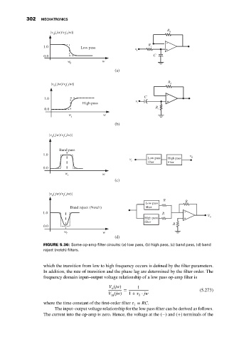
                              FIGURE 5.36: Some op-amp filter circuits: (a) low pass, (b) high pass, (c) band pass, (d) band
                              reject (notch) filters.


                              which the transition from low to high frequency occurs is defined by the filter parameters.
                              In addition, the rate of transition and the phase lag are determined by the filter order. The
                              frequency domain input–output voltage relationship of a low pass op-amp filter is
                                                         V (jw)
                                                           o          1
                                                                =                               (5.273)
                                                         V (jw)   1 +    ⋅ jw
                                                          in
                                                                      1
                              where the time constant of the first-order filter    = RC.
                                                                    1
                                   The input–output voltage relationship for the low pass filter can be derived as follows.
                              The current into the op-amp is zero. Hence, the voltage at the (−) and (+) terminals of the
   311   312   313   314   315   316   317   318   319   320   321