
Page 340 - Mechatronics with Experiments
P. 340
JWST499-Cetinkunt
JWST499-c05
326 MECHATRONICS Printer: Yet to Come October 28, 2014 11:15 254mm×178mm
LED and transistor: the forward bias voltage of the LED is V = 2.5 V, and the minimum voltage drop
f
between collector and emitter of transistor is V CE = 0.3 V (i.e., when the transistor is fully saturated),
and the gain of the transistor = 100.
6. Design an op-amp circuit to implement a PD (proportional plus derivative) control where
the proportional gain and the derivative gain are both adjustable. The circuit should have two input
voltages (V (t), V (t) and one output voltage (V (t)). The desired mathematical function to be realized
i1 i2 o
by the op-amp circuit is
V (t) = K ⋅ (V − V (t)) + K ⋅ d∕dt((V − V (t))) (5.325)
i1
p
o
i1
i2
i2
d
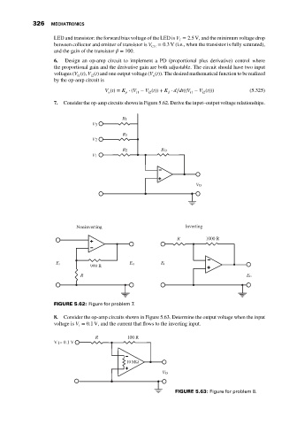
7. Consider the op-amp circuits shown in Figure 5.62. Derive the input–output voltage relationships.
RI
V3
RI
V2
RI RO
V1
–
+
VO
Noninverting Inverting
+ R 1000 R
–
–
E I EO EI
999 R +
R EO
FIGURE 5.62: Figure for problem 7.
8. Consider the op-amp circuits shown in Figure 5.63. Determine the output voltage when the input
voltage is V = 0.1 V, and the current that flows to the inverting input.
i
R 100 R
V = 0.1 V
1
−
10 MΩ
+
VO
FIGURE 5.63: Figure for problem 8.