
Page 338 - Mechatronics with Experiments
P. 338
JWST499-Cetinkunt
JWST499-c05
324 MECHATRONICS Printer: Yet to Come October 28, 2014 11:15 254mm×178mm
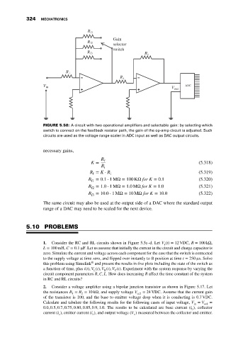
R f1
Gain
R f2
selector
switch
R f3
R i
R i
R i
V in V out ADC
FIGURE 5.58: A circuit with two operational amplifiers and selectable gain: by selecting which
switch to connect on the feedback resistor path, the gain of the op-amp circuit is adjusted. Such
circuits are used as the voltage range scaler in ADC input as well as DAC output circuits.
necessary gains,
R f
K = (5.318)
R
i
R = K ⋅ R i (5.319)
f
R = 0.1 ⋅ 1MΩ= 100 KΩ for K = 0.1 (5.320)
f1
R = 1.0 ⋅ 1MΩ= 1.0MΩ for K = 1.0 (5.321)
f2
R = 10.0 ⋅ 1MΩ= 10 MΩ for K = 10.0 (5.322)
f3
The same circuit may also be used at the output side of a DAC where the standard output
range of a DAC may need to be scaled for the next device.
5.10 PROBLEMS
1. Consider the RC and RL circuits shown in Figure 5.5c–d. Let V (t) = 12 VDC, R = 100 kΩ,
s
L = 100 mH, C = 0.1 μF. Let us assume that initially the current in the circuit and charge capacitor is
zero. Simulate the current and voltage across each component for the case that the switch is connected
to the supply voltage at time zero, and flipped over instantly to B position at time t = 250 μs. Solve
®
this problem using Simulink and present the results in five plots including the state of the switch as
a function of time, plus i(t), V (t), V (t), V (t). Experiment with the system response by varying the
L
C
R
circuit component parameters R, C, L. How does increasing R affect the time constant of the system
in RC and RL circuits?
2. Consider a voltage amplifier using a bipolar junction transistor as shown in Figure 5.17. Let
the resistances R = R = 10 kΩ, and supply voltage V cc2 = 24 VDC. Assume that the current gain
1
2
of the transistor is 100, and the base to emitter voltage drop when it is conducting is 0.7 VDC.
Calculate and tabulate the following results for the following cases of input voltage, V = V cc1 =
in
0.0, 0.5, 0.7, 0.75, 0.80, 0.85, 0.9, 1.0. The results to be calculated are base current (i ), collector
b
current (i ), emitter current (i ), and output voltage (V ) measured between the collector and emitter.
e
o
c