
Page 337 - Mechatronics with Experiments
P. 337
Printer: Yet to Come
October 28, 2014 11:15 254mm×178mm
JWST499-Cetinkunt
JWST499-c05
ELECTRONIC COMPONENTS FOR MECHATRONIC SYSTEMS 323
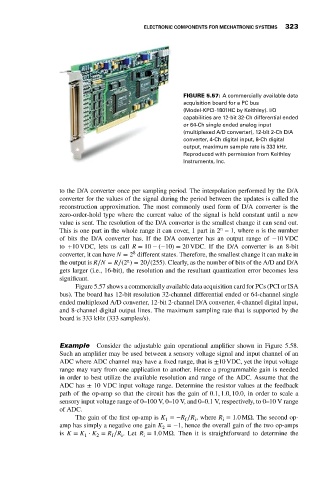
FIGURE 5.57: A commercially available data
acquisition board for a PC bus
(Model-KPCI-1801HC by Keithley). I/O
capabilities are 12-bit 32-Ch differential ended
or 64-Ch single ended analog input
(multiplexed A/D converter), 12-bit 2-Ch D/A
converter, 4-Ch digital input, 8-Ch digital
output, maximum sample rate is 333 kHz.
Reproduced with permission from Keithley
Instruments, Inc.
to the D/A converter once per sampling period. The interpolation performed by the D/A
converter for the values of the signal during the period between the updates is called the
reconstruction approximation. The most commonly used form of D/A converter is the
zero-order-hold type where the current value of the signal is held constant until a new
value is sent. The resolution of the D/A converter is the smallest change it can send out.
n
This is one part in the whole range it can cover, 1 part in 2 − 1, where n is the number
of bits the D/A converter has. If the D/A converter has an output range of −10 VDC
to +10 VDC, lets us call R = 10 − (−10) = 20 VDC. If the D/A converter is an 8-bit
8
converter, it can have N = 2 different states. Therefore, the smallest change it can make in
n
the output is R∕N = R∕(2 ) = 20∕(255). Clearly, as the number of bits of the A/D and D/A
gets larger (i.e., 16-bit), the resolution and the resultant quantization error becomes less
significant.
Figure 5.57 shows a commercially available data acquisition card for PCs (PCI or ISA
bus). The board has 12-bit resolution 32-channel differential ended or 64-channel single
ended multiplexed A/D converter, 12-bit 2-channel D/A converter, 4-channel digital input,
and 8-channel digital output lines. The maximum sampling rate that is supported by the
board is 333 kHz (333 samples/s).
Example Consider the adjustable gain operational amplifier shown in Figure 5.58.
Such an amplifier may be used between a sensory voltage signal and input channel of an
ADC where ADC channel may have a fixed range, that is ±10 VDC, yet the input voltage
range may vary from one application to another. Hence a programmable gain is needed
in order to best utilize the available resolution and range of the ADC. Assume that the
ADC has ± 10 VDC input voltage range. Determine the resistor values at the feedback
path of the op-amp so that the circuit has the gain of 0.1, 1.0, 10.0, in order to scale a
sensory input voltage range of 0–100 V, 0–10 V, and 0–0.1 V, respectively, to 0–10 V range
of ADC.
The gain of the first op-amp is K =−R ∕R , where R = 1.0MΩ. The second op-
i
1
f
i
amp has simply a negative one gain K =−1, hence the overall gain of the two op-amps
2
is K = K ⋅ K = R ∕R .Let R = 1.0MΩ. Then it is straightforward to determine the
2
1
i
i
f