
Page 339 - Mechatronics with Experiments
P. 339
Printer: Yet to Come
October 28, 2014 11:15 254mm×178mm
JWST499-Cetinkunt
JWST499-c05
ELECTRONIC COMPONENTS FOR MECHATRONIC SYSTEMS 325
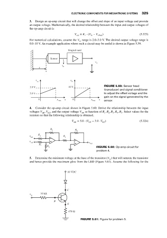
3. Design an op-amp circuit that will change the offset and slope of an input voltage and provide
an output voltage. Mathematically, the desired relationship between the input and output voltages of
the op-amp circuit is
V out = K ⋅ (V − V offset ) (5.323)
in
1
For numerical calculations, assume the V range is 2.0–3.0 V. The desired output voltage range is
in
0.0–10 V. An example application where such a circuit may be useful is shown in Figure 5.59.
Singnal card
Sensor
v
0
v
x so
v v
so 0
3.0 V 10 V FIGURE 5.59: Sensor head
(transducer) and signal conditioner
2.0 V to adjust the offset voltage and the
gain on the signal generated by the
0 x x 0 x x
max max sensor.
4. Consider the op-amp circuit shown in Figure 5.60. Derive the relationship between the input
voltages V , V , and the output voltage V as function of R , R , R , R , R . Select values for the
in1 in2 out 1 2 3 4 5
resistors so that the following relationship is obtained,
V out = 5.0 ⋅ (V in1 − 3.0 ⋅ V ) (5.324)
in2
6
3
FIGURE 5.60: Op-amp circuit for
problem 4.
5. Determine the minimum voltage at the base of the transistor (V ) that will saturate the transistor
in
and hence provide the maximum glow from the LED (Figure 5.61). Assume the following for the
10 VDC
C
v in 10 kΩ
B
E
470 Ω
FIGURE 5.61: Figure for problem 5.