
Page 334 - Mechatronics with Experiments
P. 334
JWST499-Cetinkunt
JWST499-c05
320 MECHATRONICS Printer: Yet to Come October 28, 2014 11:15 254mm×178mm
Input signal – v
v in + out
Sampled
Sample and signal
hold control
pulse v
SH
v
in
Time
v
SH
Time
v
out
Time
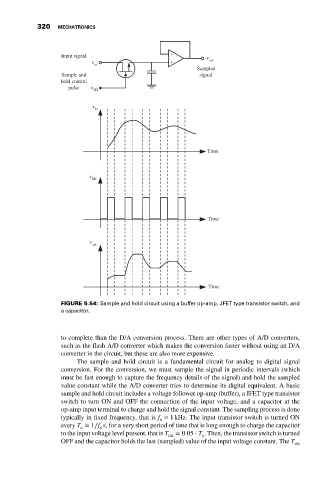
FIGURE 5.54: Sample and hold circuit using a buffer op-amp, JFET type transistor switch, and
a capacitor.
to complete than the D/A conversion process. There are other types of A/D converters,
such as the flash A/D converter which makes the conversion faster without using an D/A
converter in the circuit, but these are also more expensive.
The sample and hold circuit is a fundamental circuit for analog to digital signal
conversion. For the conversion, we must sample the signal in periodic intervals (which
must be fast enough to capture the frequency details of the signal) and hold the sampled
value constant while the A/D converter tries to determine its digital equivalent. A basic
sample and hold circuit includes a voltage follower op-amp (buffer), a JFET type transistor
switch to turn ON and OFF the connection of the input voltage, and a capacitor at the
op-amp input terminal to charge and hold the signal constant. The sampling process is done
typically in fixed frequency, that is f = 1 kHz. The input transistor switch is turned ON
s
every T = 1∕f s, for a very short period of time that is long enough to charge the capacitor
s
s
to the input voltage level present, that is T on = 0.05 ⋅ T . Then, the transistor switch is turned
s
OFF and the capacitor holds the last (sampled) value of the input voltage constant. The T on