Page 335 - Mechatronics with Experiments
P. 335

October 28, 2014 11:15 254mm×178mm
                                         Printer: Yet to Come
                        JWST499-Cetinkunt
            JWST499-c05
                                                       ELECTRONIC COMPONENTS FOR MECHATRONIC SYSTEMS  321
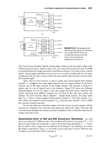
                                               Multiplexer
                             to CPU                          F       Ch1
                                        A/D                  F       Ch2
                                      converter  S&H
                                                             F       Ch3
                                                   Sample &
                                                hold circuits
                                                             F       Ch4
                                                            Anti- aliasing
                                                              filter
                                                    (a)

                                         Multiplexer
                              toCPU                  S&H     F       Ch1

                                        A/D          S&H     F       Ch2
                                      converter
                                                     S&H     F       Ch3  FIGURE 5.55: Multiplexed multi
                                                                          channel analog signal and sampling
                                           Sample &   S&H    F       Ch4  via a single A/D converter: (a)
                                        hold circuits                     multiplexed sample-and-hold
                                                            Ant i- aliasing
                                                              filter      circuit, (b) simultaneous
                                                    (b)                   sample-and-hold circuit.


                             time must be long enough so that the circuit output voltage reaches the input voltage value
                             within a desired accuracy. Typical values of T on  are in the order of microseconds. It should
                             be pointed out that the sample and hold circuit shown in Figure 5.54 is only a basic concept
                             circuit. Actual sample and hold circuits involve two or more op-amps and are a bit more
                             complicated. One op-amp is used to buffer the input and the other op-amp is used to buffer
                             the sampled output.
                                  Quite often an A/D converter is used to sample and convert signals from multiple
                             channels. A multiplexer has many input channels and one output channel. It selectively
                             connects one of the input channels to the output channel. The selection is made by a
                             digital code in a set of digital lines in the interface. Figure 5.55 shows two different
                             implementations. In case (a), there is only one sample and hold circuit. Therefore, the
                             signals converted from different channels are not taken at the same time instant. For
                             instance, the A/D converter selects channel 1, samples-hold-converts. This takes finite
                             time, T conv . Then it selects-samples-holds-converts channel 2. This takes another T conv
                             time. Hence, the channel 3 will be sampled 2 T conv  time later than channel 1. This is called
                             the sequential sample-and-hold.
                                  In case (b), there are individual sample and hold circuits for each channel. All the
                             channels are sampled at the same time and signals are held at that value. Then the A/D
                             conversion goes through each channel using the multiplexer. This is called the simultaneous
                             sample-and-hold circuit.

                             Quantization Error of A/D and D/A Converters: Resolution         An n-bit
                                                                                              n
                                               n
                             device can represent 2 different states. The resolution of the device is one part in 2 − 1. In
                                                                                           n
                             physical signal terms, the resolution is 1 part in the whole range divided by 2 − 1. Notice
                             that we need to mark a range into four discrete levels (Figure 5.56). Similarly, if we have
                                                                                   n
                                                 n
                             the ability to represent 2 states, we can divide a given range into 2 levels. Therefore, the
                             resolution of an n-bit A/D or D/A converter is
                                                                   n
                                                           V range ∕(2 − 1)                    (5.317)
   330   331   332   333   334   335   336   337   338   339   340