Page 10 - AtecomProductCatalogue
P. 10

Customized your high quality wafers


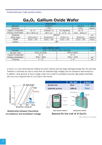
                            Ga    2O    3  Gallium Oxide Wafer

                                                       Parameters                                          Unit
               Diameter                               50.8±0.3                             100±0.5         mm
              Orientation                             <-201>                                <001>         degree
          Dopant/ Conductivity       Sn / N         Undoped / N       Fe /Insulating        Sn / N
                                                                           10
          Doping concentration  5E17~9E18 cm -3      <5E17 cm -3      R>10 Ω・cm        1E18~ 2E19 cm  -3
               Thickness                                       650±20                                      um
              Offset angle        [010]:0±0.4       [010]:0±0.4         [010]:0 ±1        [010]:0±1       degree
                FWHM              [010]:≦150        [010]:≦150         [010]:≦150         [010]:≦350      arcsec
                Surface                                           SSP


                                                   Ga 2O 3 Eptixial wafer                                  Unit
               Diameter                            50.8 ~ 100 (Ga2O3 wafer substrate)                      mm
             Epi layer Type               Ga 2 O 3  on Ga 2 O 3                 GaN on Ga 2 O 3
          Dopant/ Conductivity                Si / N                               Si / N
          Doping concentration             2E16 ~ 9E16                          1E18 ~ 1E19                cm -3
               Thickness                      5 ~ 10                                2 ~6                   um


    9
   5   6   7   8   9   10   11   12