Page 8 - AtecomProductCatalogue
P. 8

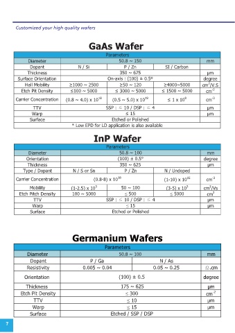
Customized your high quality wafers


                                              GaAs Wafer

                                                       Parameters
               Diameter                                      50.8 ~ 150                                   mm
                Dopant                   N / Si                 P / Zn               SI / Carbon
               Thickness                                      350 ~ 675                                   μm
          Surface Orientation                           On-axis : (100) ± 0.5º                          degree
                                                                                                           2
              Hall Mobility         ≥1000 ~ 2500              ≥50 ~ 120             ≥4000~5000          cm /V.S
            Etch Pit Density         ≤100 ~ 5000           ≤ 3000 ~ 5000           ≤ 1500 ~ 5000         cm -2
         Carrier Concentration    (0.8 ~ 4.0) x 10 18     (0.5 ~ 5.0) x 10 19         ≤ 1 x 10 8         cm -3

                  TTV                                  SSP : ≤ 10 / DSP : ≤ 4                             μm
                 Warp                                            ≤ 15                                     μm
                Surface                                   Etched or Polished
                                     * Low EPD for LD application is also available

                                                 InP Wafer

                                                       Parameters
               Diameter                                       50.8 ~ 100                                  mm
              Orientation                                    (100) ± 0.5°                               degree
               Thickness                                      350 ~ 625                                   μm
             Type / Dopant            N / S or Sn               P / Zn              N / Undoped

         Carrier Concentration                  (0.8-8) x 10 18                     (1-10) x 10 15        cm -3
                                                                                                           2
                Mobility             (1-2.5) x 10 3            50 ~ 100              (3-5) x 10 3       cm /Vs
           Etch Pitch Density         100 ~ 5000                ≤ 500                  ≤ 5000             cm 2
                  TTV                                  SSP : ≤ 10 / DSP : ≤ 4                             μm
                 Warp                                            ≤ 15                                     μm
                Surface                                   Etched or Polished


                                      Germanium Wafers


                                                      Parameters
               Diameter                                      50.8 ~ 100                                   mm
                Dopant                         P / Ga                             N / As

               Resistivity                 0.005 ~ 0.04                        0.05 ~ 0.25               Ω.cm

             Orientation                                     (100) ± 0.5                                degree

              Thickness                                       175 ~ 625                                   μm
            Etch Pit Density                                     ≤ 300                                   cm  -2
                  TTV                                            ≤ 10                                     μm
                 Warp                                            ≤ 15                                     μm
                Surface                                  Etched / SSP / DSP


    7
   3   4   5   6   7   8   9   10   11   12