
Page 7 - AtecomProductCatalogue
P. 7
ATEC M
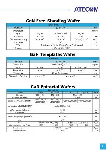
GaN Free-Standing Wafer
Parameters
Diameter 50.8~100 mm
Orientation degree
Type N / Si N / Undoped SI / Fe
Resistivity < 0.05 < 0.5 >10 6 Ω.cm
Dislocation Density <9 x 10 6 <9 x 10 6 (0.1~3) x 10 6 cm -2
Thickness 400 um
TTV Φ50.8mm:<15, Φ100mm<30 or Customized um
Surface CMP / Optical Polish
GaN Templates Wafer
Parameters
Diameter 50.8~100 mm
Orientation C-axis(0001) ± 0.5˚ degree
Type P / Mg N / Si N / Undoped
Resistivity ~10 < 0.05 < 0.5 Ω.cm
Thickness 4.5 or Customized um
Dislocation Density > 6 X 10 16 < 5 X 10 8 cm -2
GaN Epitaxial Wafers
Parameters
Substrate Silicon HR Silicon SiC Sapphire Unit
Diameter 50.8 ~ 200 150 ~ 200 50.8 ~100 mm
Epi-layer thickness >3 ~2 0.5~3 μm
<800'' (002) & <700'' (002) &
Crystalline AlGaN/GaN HEMT <250'' (2μm GaN) <400'' (2um GaN)
<2000'' (102) <1350'' (102)
Composition AlGaN/GaN HEMT Al x Ga 1-x N (0<x<0.5)
AlGaN barrier thickness 2~50 nm
AlN spacer* 0.2-2 nm
2
Surface morphology (5x5μm ) RMS<0.5 nm
Bow <50 μm
12
2DEG >9 X10 (25nm Al 0.25 GaN) >8X10 (25nm Al0.25GaN) /cm 2
12
2
2
Electron mobility (cm /Vs) >1500 >1800 >2000 >1500 cm /Vs
Sheet resistance <400(25nm Al 0.25 GaN) Ω/□
Buffer resistivity >10 5 Ω.cm
6