
Page 9 - AtecomProductCatalogue
P. 9
ATEC M
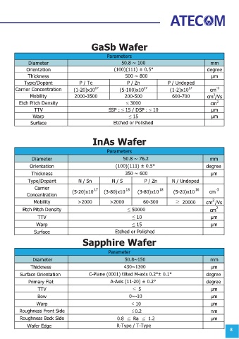
GaSb Wafer
Parameters
Diameter 50.8 ~ 100 mm
Orientation (100)(111) ± 0.5° degree
Thickness 500 ~ 800 μm
Type/Dopant P / Te P / Zn P / Undoped
Carrier Concentration (1-20)x10 17 (5-100)x10 17 (1-2)x10 17 cm -3
2
Mobility 2000-3500 200-500 600-700 cm /Vs
Etch Pitch Density ≤ 3000 cm 2
TTV SSP : ≤ 15 / DSP : ≤ 10 μm
Warp ≤ 15 μm
Surface Etched or Polished
InAs Wafer
Parameters
Diameter 50.8 ~ 76.2 mm
Orientation (100)(111) ± 0.5° degree
Thickness 350 ~ 600 μm
Type/Dopant N / Sn N / S P / Zn N / Undoped
Carrier 17 18 18 16 -3
Concentration (5-20)x10 (3-80)x10 (3-80)x10 (5-20)x10 cm
2
Mobility >2000 >2000 60-300 ≥ 20000 cm /Vs
Etch Pitch Density ≤ 50000 cm 2
TTV ≤ 10 μm
Warp ≤ 15 μm
Surface Etched or Polished
Sapphire Wafer
Parameter
Diameter 50.8~150 mm
Thickness 430~1300 μm
Surface Orientation C-Plane (0001) tilted M-axis 0.2°± 0.1° degree
Primary Flat A-Axis (11-20) ± 0.2° degree
TTV ≤ 5 μm
Bow 0~-10 μm
Warp ≤ 10 μm
Roughness Front Side ≤ 0.2 nm
Roughness Back Side 0.8 ≦ Ra ≦ 1.2 μm
Wafer Edge R-Type / T-Type
8