


Page 1096 - Basic Electrical Engineering
P. 1096
In the previous section we have seen logic gates of combinational type where
               the output at a given time depends upon the inputs at that time. The previous
               records of inputs does not effect the output at all.

                  The output of a flip-flop is either a low voltage (0) or a high voltage (1).
               The output remains in one of these states indefinitely unless an external

               trigger is applied to change that state. Thus a flip-flop will retain or remember
               a state indefinitely after the removal of the input trigger. A flip-flop is

               considered a storing device of 1-bit memory. Since a flip-flop will have two
               stable states (0 or 1), it is also referred to as bistable multivibrator.

                  In most flip-flop circuits the change of state of the flip-flop is of a definite
               rate, and hence they are of clocked type.


                                                  16.11.1 RS Flip-flop


               The RS flip-flop is used to temporarily hold or store information until it is
               required. A single RS circuit will store one binary digit, i.e., either 1 or 0. For

               storing a six digit binary number, six RS flip-flops will be required. As
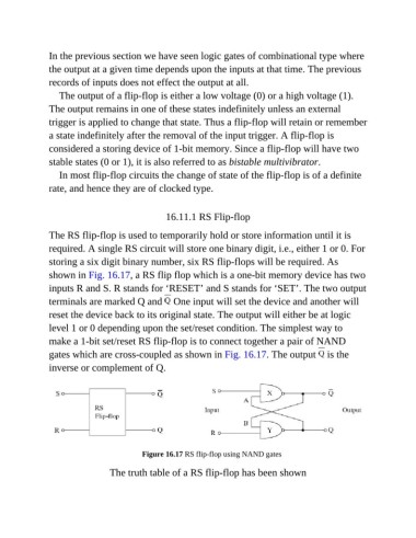
               shown in Fig. 16.17, a RS flip flop which is a one-bit memory device has two
               inputs R and S. R stands for ‘RESET’ and S stands for ‘SET’. The two output

               terminals are marked Q and   One input will set the device and another will
               reset the device back to its original state. The output will either be at logic

               level 1 or 0 depending upon the set/reset condition. The simplest way to
               make a 1-bit set/reset RS flip-flop is to connect together a pair of NAND
               gates which are cross-coupled as shown in Fig. 16.17. The output   is the

               inverse or complement of Q.


                                           Figure 16.17 RS flip-flop using NAND gates

                                 The truth table of a RS flip-flop has been shown

