


Page 1097 - Basic Electrical Engineering
P. 1097
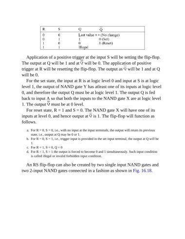
Application of a positive trigger at the input S will be setting the flip-flop.
               The output at Q will be 1 and at   will be 0. The application of positive

               trigger at R will be resetting the flip-flop. The output as   will be 1 and at Q
               will be 0.

                  For the set state, the input at R is at logic level 0 and input at S is at logic
               level 1, the output of NAND gate Y has atleast one of its inputs at logic level

               0, and therefore the output Q must be at logic level 1. The output Q is fed
               back to input A so that both the inputs to the NAND gate X are at logic level
               1. The output   must be at 0 level.

                  For reset state, R = 1 and S = 0. The NAND gate X will have one of its
               inputs at level 0, and hence output at   is 1. The flip-flop will function as

               follows.

                   a.  For R = 0, S = 0, i.e., with no input at the input terminals, the output will retain its previous
                     state, i.e., output at Q may be 0 or 1.
                   b.  For R = 0, S = 1, i.e., trigger input is provided in the set input terminal, the output at Q will be
                     1.
                   c.  For R = 1, S = 0, Q = 0
                   d.  For R = 1, S = 1 the output is forced to become 0 and 1 simultaneously. Such input condition
                     is called illegal or invalid forbidden input condition.


                  An RS flip-flop can also be created by two single input NAND gates and
               two 2-input NAND gates connected in a fashion as shown in Fig. 16.18.

