
Page 183 - Fiber Optic Communications Fund
P. 183
164 Fiber Optic Communications
FSK signal
m(t) m'(t) s(t) = Aexp[i2π(f t + k m'(t))]
Integrator PM c f
10 1 1 1 1 0 1 1 1
Field
t t
t
T b T b
Laser
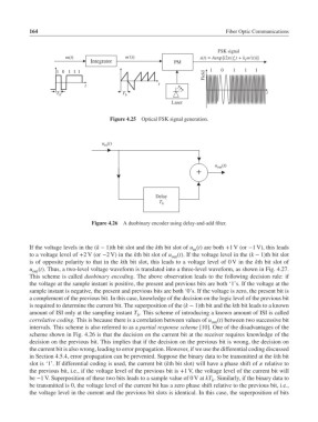
Figure 4.25 Optical FSK signal generation.
u in (t)
u out (t)
+
Delay
T b
Figure 4.26 A duobinary encoder using delay-and-add filter.
If the voltage levels in the (k − 1)th bit slot and the kth bit slot of u (t) are both +1 V (or −1 V), this leads
in
to a voltage level of +2 V (or −2 V)inthe kth bit slot of u (t). If the voltage level in the (k − 1)th bit slot
out
is of opposite polarity to that in the kth bit slot, this leads to a voltage level of 0 V in the kth bit slot of
u (t). Thus, a two-level voltage waveform is translated into a three-level waveform, as shown in Fig. 4.27.
out
This scheme is called duobinary encoding. The above observation leads to the following decision rule: if
the voltage at the sample instant is positive, the present and previous bits are both ‘1’s. If the voltage at the
sample instant is negative, the present and previous bits are both ‘0’s. If the voltage is zero, the present bit is
a complement of the previous bit. In this case, knowledge of the decision on the logic level of the previous bit
is required to determine the current bit. The superposition of the (k − 1)th bit and the kth bit leads to a known
amount of ISI only at the sampling instant T . This scheme of introducing a known amount of ISI is called
b
correlative coding. This is because there is a correlation between values of u (t) between two successive bit
out
intervals. This scheme is also referred to as a partial response scheme [10]. One of the disadvantages of the
scheme shown in Fig. 4.26 is that the decision on the current bit at the receiver requires knowledge of the
decision on the previous bit. This implies that if the decision on the previous bit is wrong, the decision on
the current bit is also wrong, leading to error propagation. However, if we use the differential coding discussed
in Section 4.5.4, error propagation can be prevented. Suppose the binary data to be transmitted at the kth bit
slot is ‘1’. If differential coding is used, the current bit (kth bit slot) will have a phase shift of relative to
the previous bit, i.e., if the voltage level of the previous bit is +1 V, the voltage level of the current bit will
be −1 V. Superposition of these two bits leads to a sample value of 0 V at kT . Similarly, if the binary data to
b
be transmitted is 0, the voltage level of the current bit has a zero phase shift relative to the previous bit, i.e.,
the voltage level in the current and the previous bit slots is identical. In this case, the superposition of bits