Page 220 - Fiber Optic Communications Fund
P. 220

Optical Receivers                                                                  201


           5.2.5  Speed or Response Time
           The speed of response or bandwidth of a pin photodetector, shown in Fig. 5.8, depends on the following
           factors.

           1. The transit time  of the photogenerated carriers through the depletion or active region, given by
                           t
                                                        W
                                                     =  ,                                 (5.26)
                                                    t
                                                        
             where  is the speed of the carrier. If the carriers are not traveling at their saturation velocity  , then
                                                                                          sat
              = E where  is the mobility of the carrier traveling in an electric field E. The electric field intensity
             is in turn computed from E ∼ V∕W, where V is the voltage across the depletion region W. Therefore, we
             can write  as
                      t
                              {
                                W∕ , for carriers traveling at their saturation velocity
                                    sat
                           =                                                              (5.27)
                           t
                                  2
                                W ∕(μV), for carriers traveling below their saturation velocity.
           2. The slower (relative to drifting carriers) diffusion of carriers occurs outside the depletion region. To min-
             imize this diffusion time effect, generally the depletion region is made as large as possible. For example,
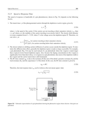
             a pin photodiode (Fig. 5.8) may be used instead of a pn photodiode where the i-region is much larger
             than a typical reverse-biased depletion region. Also, because the doping concentration in the i-region is
             significantly lower than that in the p- or n-regions in a pin photodiode, then most of the depletion width is
             the i-region and the carrier transit time is drift dominated.
           3. The RC time constant   is due to the resistance R (the sum of the diode’s parasitic resistance R and the
                                RC                                                        S
             load resistance R ) and the capacitance C of the diode. In this case, the RC time constant is given by
                           L
                                                    RC  = RC.                             (5.28)

             Therefore, the total response time  tot  can be written as the root-mean-square value
                                                     √
                                                             2
                                                        2
                                                 tot  =   RC  +  .                    (5.29)
                                                             t


                                                                p +


                                                                  +
                                     Reverse-bias
                                      voltage V R                 ‒
                                                             i-layer

                                                                n +
                                                    Load resistor R L


           Figure 5.8  Schematic representation of a pin photodiode showing the photoactive region where electron–hole pairs are
           generated.
   215   216   217   218   219   220   221   222   223   224   225