
Page 223 - Fiber Optic Communications Fund
P. 223
204 Fiber Optic Communications
than 100 GHz [6] by using a matching network and decreasing the device size, but this reduces the quantum
efficiency. If a side-entry or a waveguide-fed pin-PD is fabricated, then the -BW product can be further
improved [7].The -BW product can also be increased by inserting the pin-PD inside a resonant cavity as
in RCE-PDs, where the quantum efficiency is enhanced even for a thin absorption layer due to reflections
of light through the bottom and top mirrors of the cavity, resulting in multi-passes of light through the
absorption layer. This is discussed in more detail later in section 5.3.8.1.
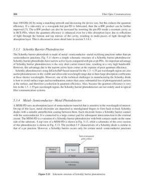
5.3.3 Schottky Barrier Photodetector
The Schottky barrier photodiode is made of metal–semiconductor–metal rectifying junctions rather than pn
semiconductor junctions. Fig. 5.11 shows a simple schematic structure of a Schottky barrier photodetector.
Schottky barrier photodiodes have narrow active layers compared with pin or pn PDs. An important advantage
of Schottky barrier photodetectors is the very short carrier transit time, resulting in a very high bandwidth.
However, this advantage due to the narrow active layer comes at the expense of poor quantum efficiency.
Schottky photodetectors using InGaAs/InP-based material for the 1.3–1.55 μm wavelength region are also
useful photodetectors in the visible and ultraviolet wavelength range due to their large absorption coefficients
at these shorter wavelengths. However, one of the technical challenges in manufacturing the Schottky diode
is how to avoid surface traps and recombination centers that cause substantial loss of photogenerated carriers
at the surface, and therefore a reduction in quantum efficiency. Also, because the quantum efficiency is very
low in the 1.3–1.55 μm wavelength region, the Schottky barrier photodetectors are not widely used in optical
fiber communication systems.
5.3.4 Metal–Semiconductor–Metal Photodetector
A MSM-PD uses an absorption layer of semiconductor material that is sensitive to the wavelength of interest.
On top of this layer, metal electrodes are deposited as interdigitated fingers to form back-to-back Schottky
diodes with a suitable antireflection coating between them. Each electrode forms a Schottky barrier contact
with the semiconductor. It is connected to a large contact pad for subsequent interconnection to the external
circuit. The MSM-PD is a variation of a Schottky barrier photodetector with both contacts made on the same
side of the substrate. A top view of a MSM-PD is shown in Fig. 5.12, while a schematic of the cross-section
of this photodetector is shown in Fig. 5.13. The rectified I-V characteristic of a Schottky diode is similar to
that of a pn junction. However, a Schottky barrier occurs only for certain metal–semiconductor junctions
Semi-transparent
gold contact
Metal-n + n layer Metal-n +
‒
contact contact
+
n layer
Semi-insulating
substrate
Figure 5.11 Schematic structure of Schottky barrier photodetector.