
Page 228 - Fiber Optic Communications Fund
P. 228
Optical Receivers 209
( )
R r0e;h
= tanh ,
e;h 0e;h
2kT
( )
R r0e;h
E re;h = E r0e;h tanh ,
2kT
where 0e;h , E r0e;h , and k are the carrier mean free path at T = 0 K, average energy loss per collision for an
electron and a hole, respectively, and Boltzmann’s constant. E is the semiconductor (e.g., InP) band gap, and
g
E ie0 and E ih0 are the electron and hole ionization energies at 0 K. From Eq. (5.34), the breakdown conditions
are expected to be temperature independent in the low-temperature limit.
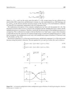
The mathematical description of the avalanche multiplication has been well documented [21–24].The
theoretical research in these reviews is based on the assumption that the multiplication layer is thick, and the
multiplication process is continuous. Therefore, statistically, the discrete nature of the multiplication process is
averaged out. This is reflected, for example, in the fact that there is no “dead” space–a space where ionization
is impossible because the carrier has not acquired enough energy to initiate the multiplication process. Under
these assumptions, the multiplication occurs only in the multiplication region of thickness W (between 0 and
W). For details, see Fig. 5.16.
The electron component J (x) of the total current increases, and the hole component J (x) of the total current
n p
decreases along the positive x-direction. The rate equation for J (x) and J (x) in this case can be written as
n p
d
J (x)= (x) ⋅ J (x)+ (x) ⋅ J (x)+ q ⋅ G(x), (5.35)
n
n
p
dx
d
− J (x)= (x) ⋅ J (x)+ (x) ⋅ J (x)+ q ⋅ G(x), (5.36)
p
p
n
dx
electric field
J (0) J n (W)
n
P N
J p (0) J p (W)
x
0 W
(a)
M(x)
M n M p
> >
M n M p
x
0 W
(b)
Figure 5.16 (a) Avalanche multiplication within a multiplication region of thickness W and (b) gain along the x-direction
for the cases > and < .