
Page 224 - Fiber Optic Communications Fund
P. 224
Optical Receivers 205
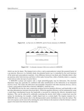
Schottky Contacts
Schottky Contacts
(a) (b)
Figure 5.12 (a) Top view of a MSM-PD. and (b) Circuit schematic of a MSM-PD.
Schottky contacts
Undoped active layer
Semi-insulating substrate
Figure 5.13 A schematic structure of the cross-section of a MSM-PD.
which can also be ohmic. The doping levels in the p- and n-semiconductors control the potential barrier of
a pn junction. However, in a Schottky diode, the potential barrier ( ) is controlled by the work functions
b
of the metal and semiconductor materials. A key difference between a pn diode and a Schottky diode is that
pn junctions allow both electrons and holes to flow under forward bias, while a Schottky diode is a majority
carrier device (only one type of carrier flows).
A MSM-PD is planar and requires only a single photolithography step for fabrication. The electrode
deposition stage may generally be combined with other metallizations in the fabrication of an integrated
receiver circuit. This makes the fabrication and monolithic integration with other electronic devices, such as
a metal–semiconductor field-effect transistor (MESFET), relatively easy.
The MSM-PD also has the same compromise problem between quantum efficiency and bandwidth as with
the other photodetector structures discussed above. While the quantum efficiency can be maintained by using
a multi-finger interdigitated layout, the bandwidth is increased by reducing the effective absorption layer
thickness. This can be achieved by artificially restricting the electric field within a certain layer near the
surface by introducing, for example, a highly doped layer at a certain depth. The impulse response for a
MSM-PD shows a tail response due to the photogenerated carrier distribution away from the surface. The
slow tail response can be removed by tailoring the carrier lifetime in the material so that the lifetime is almost
equal to the transit time between the electrodes.