
Page 226 - Fiber Optic Communications Fund
P. 226
Optical Receivers 207
Optical
input
AR coating Metal
n InP emitter
InGaAs base
n InP collector
n InP substrate
Metal
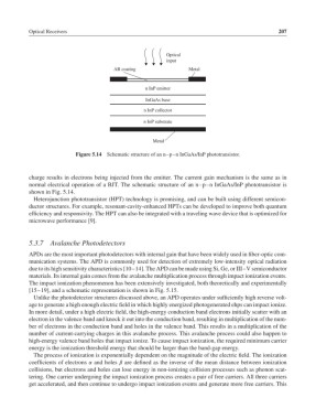
Figure 5.14 Schematic structure of an n–p–n InGaAs/InP phototransistor.
charge results in electrons being injected from the emitter. The current gain mechanism is the same as in
normal electrical operation of a BJT. The schematic structure of an n–p–n InGaAs/InP phototransistor is
shown in Fig. 5.14.
Heterojunction phototransistor (HPT) technology is promising, and can be built using different semicon-
ductor structures. For example, resonant-cavity-enhanced HPTs can be developed to improve both quantum
efficiency and responsivity. The HPT can also be integrated with a traveling wave device that is optimized for
microwave performance [9].
5.3.7 Avalanche Photodetectors
APDs are the most important photodetectors with internal gain that have been widely used in fiber-optic com-
munication systems. The APD is commonly used for detection of extremely low-intensity optical radiation
due to its high sensitivity characteristics [10–14]. The APD can be made using Si, Ge, or III–V semiconductor
materials. Its internal gain comes from the avalanche multiplication process through impact ionization events.
The impact ionization phenomenon has been extensively investigated, both theoretically and experimentally
[15–19], and a schematic representation is shown in Fig. 5.15.
Unlike the photodetector structures discussed above, an APD operates under sufficiently high reverse volt-
age to generate a high enough electric field in which highly energized photogenerated ehps can impact ionize.
In more detail, under a high electric field, the high-energy conduction band electrons initially scatter with an
electron in the valence band and knock it out into the conduction band, resulting in multiplication of the num-
ber of electrons in the conduction band and holes in the valence band. This results in a multiplication of the
number of current-carrying charges in this avalanche process. This avalanche process could also happen to
high-energy valence band holes that impact ionize. To cause impact ionization, the required minimum carrier
energy is the ionization threshold energy that should be larger than the band-gap energy.
The process of ionization is exponentially dependent on the magnitude of the electric field. The ionization
coefficients of electrons and holes are defined as the inverse of the mean distance between ionization
collisions, but electrons and holes can lose energy in non-ionizing collision processes such as phonon scat-
tering. One carrier undergoing the impact ionization process creates a pair of free carriers. All three carriers
get accelerated, and then continue to undergo impact ionization events and generate more free carriers. This