
Page 231 - Fiber Optic Communications Fund
P. 231
212 Fiber Optic Communications
Optical input
AR coating
Dielectric ‒
+
p InP
Guard ring
n InP multiplication
n InGaAs absorption
n InP buffer
+
n InP substrate
Metal contact
(a)
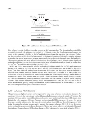
Figure 5.17 (a) Schematic structure of a planar SAM InP/InGaAs APD.
bias voltages to avoid significant tunneling currents at this heterointerface. The absorption layer should be
completely depleted with minimum electric field of 10 V/μm to ensure that the photogenerated carriers are
swept at their saturated velocities to the InP multiplication region at the operating bias voltages. Further,
the absorption layer width should be large enough to obtain good quantum efficiency by ensuring adequate
absorption, but not too large so as to increase unnecessarily the carrier transit time and reduce the bandwidth.
The maximum electric field in the InP multiplication layer should be larger than 45 V/μm to achieve significant
avalanche multiplication. And the doping concentration in the InP multiplication layer should be smaller than
17
2 × 10 cm −3 to avoid the large tunneling current [25, 26].
In [11] and [21], a manufacturable bulk InP avalanche photodiode suitable for 10-Gb/s applications was
introduced. It builds on the SAM structure with a bulk InP multiplication layer and an InGaAs absorption
layer. Then, three InGaAsP grading layers between the field control and absorption layer are included to
minimize hole trapping resulting from the valence band discontinuity that forms at an InGaAs–InP het-
erointerface. Also, edge breakdown is controlled by shaping the diffusion profile using a double-diffusion
technique to create a wider multiplication region with a higher breakdown voltage around the device periph-
ery. The back-illuminated geometry minimizes capacitance and dark current for a given optical coupling
diameter. This separate absorption, grading, charge, and multiplication (SAGCM) APD structure is one in
which the absorption, grading, charge, and absorption layers occur in sequence, as shown in Fig. 5.18, and it
has excellent optoelectronic performance characteristics.
5.3.8 Advanced Photodetectors *
The performance of photoreceivers can be improved by using some advanced photodetector structures. As
mentioned before, in the conventional surface-illuminated photodetectors, there is a trade-off between the
quantum efficiency and the bandwidth as thinner absorption layer results in a higher bandwidth (transit-time
limited) but a low quantum efficiency. Resonant cavity-enhanced (RCE) structures with a very thin active
layer are a possible solution as the thin layer gives rise to a large bandwidth, and the multiple passes of light
in the absorption layer in the resonant cavity increase the quantum efficiency [28–34]. A thin absorption
region is placed in an asymmetric Fabry–Prot cavity. The top and bottom reflectors, which can be fabricated
by distributed Bragg reflectors (DBRs), form the cavity. This is discussed in more detail in Section 5.3.8.1.