
Page 232 - Fiber Optic Communications Fund
P. 232
Optical Receivers 213
p-metal
SiO 2 AR SiO 2
+
p InP diffused x j
Energy (a.u.)
‒
n InP multiplication x d
t mesa
t
+
n InP charge InP
n InGaAs grading t g
n InGaAs t h
‒
n InGaAs
t Conduction band
absorption absorp Valence band
t und
‒
n InP buffer t buff Distance level Fenni
y active
y periphery
+
n InP substrate
(a) (b)
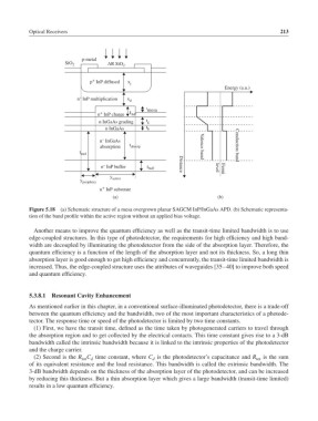
Figure 5.18 (a) Schematic structure of a mesa overgrown planar SAGCM InP/InGaAs APD. (b) Schematic representa-
tion of the band profile within the active region without an applied bias voltage.
Another means to improve the quantum efficiency as well as the transit-time limited bandwidth is to use
edge-coupled structures. In this type of photodetector, the requirements for high efficiency and high band-
width are decoupled by illuminating the photodetector from the side of the absorption layer. Therefore, the
quantum efficiency is a function of the length of the absorption layer and not its thickness. So, a long thin
absorption layer is good enough to get high efficiency and concurrently, the transit-time limited bandwidth is
increased. Thus, the edge-coupled structure uses the attributes of waveguides [35–40] to improve both speed
and quantum efficiency.
5.3.8.1 Resonant Cavity Enhancement
As mentioned earlier in this chapter, in a conventional surface-illuminated photodetector, there is a trade-off
between the quantum efficiency and the bandwidth, two of the most important characteristics of a photode-
tector. The response time or speed of the photodetector is limited by two time constants.
(1) First, we have the transit time, defined as the time taken by photogenerated carriers to travel through
the absorption region and to get collected by the electrical contacts. This time constant gives rise to a 3-dB
bandwidth called the intrinsic bandwidth because it is linked to the intrinsic properties of the photodetector
and the charge carrier.
(2) Second is the R C time constant, where C is the photodetector’s capacitance and R is the sum
tot d d tot
of its equivalent resistance and the load resistance. This bandwidth is called the extrinsic bandwidth. The
3-dB bandwidth depends on the thickness of the absorption layer of the photodetector, and can be increased
by reducing this thickness. But a thin absorption layer which gives a large bandwidth (transit-time limited)
results in a low quantum efficiency.