Page 237 - Fiber Optic Communications Fund
P. 237

218                                                               Fiber Optic Communications


                                                        W
                                           100  10   1    0.1  0.01  0.001
                10                                                                             10
                                    RCE max                  RCE max                  RCE max
                     R 2  = 1       no RCE    R 2  = 0.9     no RCE    R 2  = 0.8     no RCE
                                    RCE min                  RCE min                  RCE min
                 1  R 1  = 0                 R  = 0                   R  = 0                   1
              Quantum efficiency  0.1  R 1  = 0.70  R 1  = 0.70       R 1  = 0.70              0.1
                                                                       1
                                              1
                                                                      R 1  = 0.50
                                             R 1  = 0.50
                    R 1  = 0.50
                    R 1  = xx
                                                                      R 1  = xx
                                             R 1  = xx
               0.01  R 1  = xx               R 1  = xx                R 1  = xx                0.01

              0.001                                                                            0.001
                 100   10   1    0.1  0.01  0.001                   100  10   1    0.1  0.01  0.001
                               W                                               W

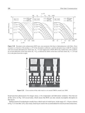
            Figure 5.20  Resonant cavity enhancement (RCE max, non-monotonic thin lines) of photodetectors with Fabry–Perot
            resonator as a function of the product  × W of the absorption coefficient  and the absorption layer width W compared
            with non-resonant photodetectors (thick lines, R = 0) and suppression in RCE (RCE min, dashed lines with symbols)
                                               2
            for several reflections of the front mirror (R = R , as indicated by labels on the lines) and back mirror (R = 1, 0.9 and
                                            1   S                                       2
            0.8, in the plots from left to right).


                                  ˜10 μm


                        Figure 5.21 Cross-section of the oxide stack in a six-metal CMOS, around year 2000.


            broad-spectrum photosensors for imager arrays, or by temperature and fabrication variations. Note that not
            all the curves in Fig. 5.20 exceed unity, which means that RCE can only remedy incomplete absorption in
            thin layers.
              Submicrometer Si technologies usually have a thick stack of oxide layers, in the range of 3–10 μmasshown
            in Fig. 5.21 from Ref. [43], since many metal layers need to be accommodated for electrical interconnections.
   232   233   234   235   236   237   238   239   240   241   242