
Page 238 - Fiber Optic Communications Fund
P. 238
Optical Receivers 219
μm ε r 1
0.60 7.5 0.8
0.75 4.2
1.00 4.2 0.6
0.35 4.2 0.4 One uniform dielectric layer
1.10 3.7 0.2
0.20 4.2
1.10 3.7 Transmittance as External Quantum Efficiency 0 400 450 500 550 600 650 700 750 800
0.20 4.2 ≈ 9.5 μm physical ≈19 μm optical 1
1.10 3.7
0.20 4.2 0.8
1.10 3.7 0.6
0.2 4.2 0.4
1.10 3.7
0.2 Twelve dielectric layers
0.75 4.0
p + n + 0
11.0 400 450 500 550 600 650 700 750 800
Wavelength (λ, nm)
(a) (b)
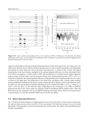
Figure 5.22 Layer content corresponding to Fig. 5.21 around year 2000. (a) Thicknesses (in microns) and relative
permittivity of the layers. (b) Transmittance of the dielectric stack calculated at assumptions for uniform (upper plot) and
alternated (bottom plot) refractive index.
Apart from the problem of having an unobstructed optical path in the web of metal wires, the oxide stack is not
uniform but alternate silicon nitride and silicon dioxide layers in order to enable nanometer-scale lithography
and etching for metal wires and vias for electrical interconnection, as shown in Fig. 5.22(a). The optical
transmittance of the stack, being a multiplier in the external quantum efficiency, has been calculated in Ref.
[43] with two assumptions, as shown in Fig. 5.22(b). One assumption is to consider a nearly uniform dielectric
√ √
with an average refractive index, since the majority of layers have similar permittivity, thus 4.2 ≈ 3.7 ≈ 2.
Using this assumption, the external quantum efficiency of the photodetector is undulating between two values,
as shown in the upper plot. The bottom plot is the result from calculation with a transfer matrix method,
showing additional modulation with slowly varying components due to thinner cavities in the dielectric stack.
2
In either case, the spacing between minima and maxima can be estimated by FSR =( ∕L ), where L ≈
opt opt
(ΣnL)≈ 19.5 μm, here, n is the refractive index. Depending on the wavelength , the values of FSR are
between 9 nm and 32 nm. These values are relatively small for broadband light in natural scenes. Thus, the
RCE effects do not compromise the use of CMOS technology for imager arrays. However, for special cases
in spectrometry, it is clear that standard CMOS may not be the best choice.
5.4 Direct Detection Receivers
Fig. 5.23 shows the block diagram of a digital optical receiver. It has three parts: (i) front end, (ii) linear chan-
nel, and (iii) data recovery section (see Ref. [3] for more details). The front end consists of a reverse-biased
photodiode. The photodiode converts the optical data into electrical data. The output of the photodiode passes
through a preamplifier.