
Page 240 - Fiber Optic Communications Fund
P. 240
Optical Receivers 221
5.4.1.1 pin-HEMT
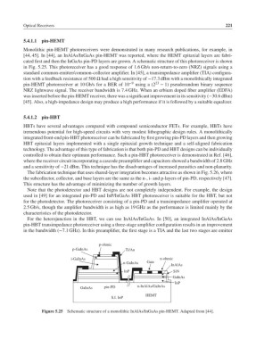
Monolithic pin-HEMT photoreceivers were demonstrated in many research publications, for example, in
[44, 45].In [44], an InAlAs/InGaAs pin-HEMT was reported, where the HEMT epitaxial layers are fabri-
cated first and then the InGaAs pin-PD layers are grown. A schematic structure of this photoreceiver is shown
in Fig. 5.25. This photoreceiver has a good response of 1.6 Gb/s non-return-to-zero (NRZ) signals using a
standard common-emitter/common-collector amplifier. In [45], a transimpedance amplifier (TIA) configura-
tion with a feedback resistance of 500 Ω had a high sensitivity of −17.3 dBm with a monolithically integrated
23
pin-HEMT photoreceiver at 10 Gb/s for a BER of 10 −9 using a (2 − 1) pseudorandom binary sequence
NRZ lightwave signal. The receiver bandwidth is 7.4 GHz. When an erbium doped fiber amplifier (EDFA)
was inserted before the pin-HEMT receiver, there was a significant improvement in its sensitivity (−30.6 dBm)
[45]. Also, a high-impedance design may produce a high performance if it is followed by a suitable equalizer.
5.4.1.2 pin-HBT
HBTs have several advantages compared with compound semiconductor FETs. For example, HBTs have
tremendous potential for high-speed circuits with very modest lithographic design rules. A monolithically
integrated front-end pin-HBT photoreceiver can be fabricated by first growing pin-PD layers and then growing
HBT epitaxial layers implemented with a single epitaxial growth technique and a self-aligned fabrication
technology. The advantage of this type of fabrication is that both pin-PD and HBT designs can be individually
controlled to obtain their optimum performance. Such a pin-HBT photoreceiver is demonstrated in Ref. [46],
where the receiver circuit incorporating a cascode preamplifier and capacitors showed a bandwidth of 2.8 GHz
and a sensitivity of −21 dBm. This technique has the disadvantages of increased parasitics and non-planarity.
The fabrication technique that uses shared-layer integration becomes attractive as shown in Fig. 5.26, where
the subcollector, collector, and base layers are the same as the n-, i- and p-layers of pin-PD, respectively [47].
This structure has the advantage of minimizing the number of growth layers.
Note that the photodetector and HBT designs are not completely independent. For example, the design
used in [49] for an integrated pin-PD and InP/InGaAs HBT photoreceiver is suitable for the HBT, but not
for the photodetector. The photoreceiver consisting of a pin-PD and a transimpedance amplifier operated at
2.5 Gb/s, though the amplifier bandwidth is as high as 19 GHz as the performance is limited mainly by the
characteristics of the photodetector.
For the heterojunction in the HBT, we can use InAlAs/InGaAs. In [50], an integrated InAlAs/InGaAs
pin-HBT transimpedance photoreceiver using a three-stage amplifier configuration results in an improvement
in the bandwidth (∼7.1 GHz). In this preamplifier, the first stage is a TIA and the last two stages are emitter
p-ohmic
p-GaInAs Ti/Au
i-GaInAs n-ohmic
n-GaInAs Gate
InAlAs
InP SiN
GaInAs
InP
GaInAs pin-PD n-InAlAs/GaInAs
HEMT
S.I. InP
Figure 5.25 Schematic structure of a monolithic InAlAs/InGaAs pin-HEMT. Adapted from [44].