
Page 242 - Fiber Optic Communications Fund
P. 242
Optical Receivers 223
18 ‒3
8nm InGaAs:5 × 10 cm 50nm i-InAlAs
2.5nm i-AlAs etch 50nm i-InAlGaAs (graded)
17nm i-InAlAs 1μm InGaAs absorption
HEMT 5nm i-InAlAs 100nm InP:Fe
MSM
18
‒3
20nm i-InGaAs 8nm InGaAs:5 × 10 cm Si
5nm i-InAlAs 2.5nm i-AlAs etch stop
25nm i-InAlAs:Fe 17nm i-InAlAs
1μm InP:Fe barrier/etch 5nm i-InAlAs
MSM 5nm i-InGaAs etch 20nm i-InGaAs
50nm i- HEMT 5nm i-InAlAs
50nm i-InAlGaAs 25nm i-InAlAs:Fe
1μm InGaAs 50nm InP:Fe
50nm InP:Fe InP:Fe substrate
InP:Fe substrate
(a) (b)
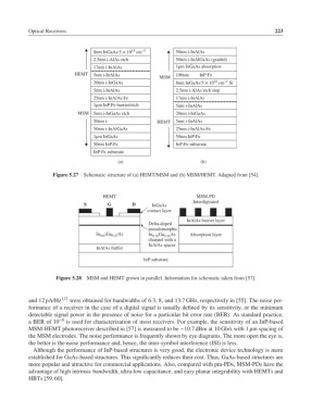
Figure 5.27 Schematic structure of (a) HEMT/MSM and (b) MSM/HEMT. Adapted from [54].
HEMT MSM-PD
Interdigitated
S G D InGaAs
contact layer
InAlAs barrier layer
Delta-doped
pseudomorphic
In 0.63 Ga 0.47 As In 0.76 Ga 0.26 As Absorption layer
channel with a
InAlAs spacer
InAlAs buffer
InP substrate
Figure 5.28 MSM and HEMT grown in parallel. Information for schematic taken from [57].
and 12 pA/Hz 1∕2 were obtained for bandwidths of 6.3, 8, and 13.7 GHz, respectively in [55]. The noise per-
formance of a receiver in the case of a digital signal is usually defined by its sensitivity, or the minimum
detectable signal power in the presence of noise for a particular bit error rate (BER). As standard practice,
a BER of 10 −9 is used for characterization of most receivers. For example, the sensitivity of an InP-based
MSM-HEMT photoreceiver described in [57] is measured to be −10.7 dBm at 10 Gb/s with 1 μm spacing of
the MSM electrodes. The noise performance is frequently shown by eye diagrams. The more open the eye is,
the better is the noise performance and, hence, the inter-symbol interference (ISI) is less.
Although the performance of InP-based structures is very good, the electronic device technology is more
established for GaAs-based structures. This significantly reduces their cost. Thus, GaAs-based structures are
more popular and attractive for commercial applications. Also, compared with pin-PDs, MSM-PDs have the
advantage of high intrinsic bandwidth, ultra-low capacitance, and easy planar integrability with HEMTs and
HBTs [59, 60].