
Page 222 - Fiber Optic Communications Fund
P. 222
Optical Receivers 203
5.3.1 pn Photodiode
A pn photodiode is basically a pn junction diode operating under reverse bias. It has already been described
in Section 5.2.1 and Fig. 5.5. In a pn photodiode, the incident photons may be absorbed in both depletion
and diffusion regions, and the number of ehps generated is proportional to the optical power (see Eqs. (5.11)
and (5.16)). The ehps are separated in the depletion region and are induced to drift under the influence of
the external applied electric field. In designing a pn photodiode, the depletion or absorption region should be
wide enough to achieve high quantum efficiency, but at the same time, it should not be too wide because the
drift time increases with the width, resulting in a decrease of the bandwidth of the photodiode. As mentioned
before, this exemplifies the compromise between quantum efficiency and speed for almost all photodetectors.
5.3.2 pin Photodetector (pin-PD)
The pin photodetector is one of the popular types used in fiber-optic communications and it was previously
introduced in Section 5.2.5. The performance of pin-PDs surpasses that of pn photodiodes because they can
easily be tailored for optimum quantum efficiency and bandwidth (see the sensitivity–bandwidth trade-off
+
+
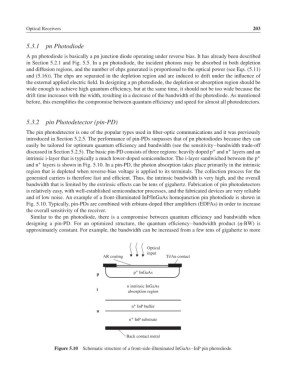
discussed in Section 5.2.5). The basic pin-PD consists of three regions: heavily doped p and n layers and an
intrinsic i-layer that is typically a much lower-doped semiconductor. The i-layer sandwiched between the p +
+
and n layers is shown in Fig. 5.10. In a pin-PD, the photon absorption takes place primarily in the intrinsic
region that is depleted when reverse-bias voltage is applied to its terminals. The collection process for the
generated carriers is therefore fast and efficient. Thus, the intrinsic bandwidth is very high, and the overall
bandwidth that is limited by the extrinsic effects can be tens of gigahertz. Fabrication of pin photodetectors
is relatively easy, with well-established semiconductor processes, and the fabricated devices are very reliable
and of low noise. An example of a front-illuminated InP/InGaAs homojunction pin photodiode is shown in
Fig. 5.10. Typically, pin-PDs are combined with erbium-doped fiber amplifiers (EDFAs) in order to increase
the overall sensitivity of the receiver.
Similar to the pn photodiode, there is a compromise between quantum efficiency and bandwidth when
designing a pin-PD. For an optimized structure, the quantum efficiency–bandwidth product (-BW) is
approximately constant. For example, the bandwidth can be increased from a few tens of gigahertz to more
Optical
input
AR coating Ti/Au contact
+
p InGaAs
p
n intrinsic InGaAs
i absorption region
+
n InP buffer
n
+
n InP substrate
Back contact metal
Figure 5.10 Schematic structure of a front-side-illuminated InGaAs–InP pin photodiode.