
Page 256 - Fiber Optic Communications Fund
P. 256
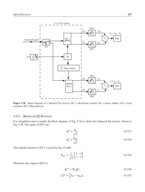
Optical Receivers                                                                  237


                                           2 × 4  90° hybrid
                                                                  PD1
                                                             1
                                                             q out      I Q+
                                                                                 I  = I Q+  −I Q−
                                                                                 Q
                                                                          +
                                                                             Σ
                                                DC 1                                 ESP
                   Received signal
                                                             2            ‒
                                                             q out      I Q−
                                  PS
                                                                  PD2
                    LO                           PS


                                             π
                                                Phase-shifter
                                             2
                                                                   PD3
                                                             3
                                                             q out      I I+
                                                                                 I  = I −I I−
                                                                                    I+
                                                                                 I
                                                                          +
                                                  DC 2                       Σ       ESP
                                                             4            ‒
                                                             q out      I I−
                                                                   PD4
           Figure 5.38  Block diagram of a balanced IQ receiver. DC = directional coupler, PS = power splitter, LO = local
           oscillator, PD = Photodetector.


           5.6.4  Balanced IQ Receiver

           It is straightforward to modify the block diagram of Fig. 5.36 to obtain the balanced IQ receiver, shown in
           Fig. 5.38. The inputs of DC1 are
                                                       q
                                                  in    r
                                                 q = √ ,                                   (5.127)
                                                  1
                                                        2
                                                      q LO
                                                  in
                                                 q = √ .                                   (5.128)
                                                  2
                                                        2
           The transfer function of DC1 is given by Eq. (5.106),
                                                       [    ]
                                                    1   1 −i
                                             T                .                            (5.129)
                                              DC  = √   −i 1
                                                     2
           Therefore, the output of DC1 is
                                                          in
                                                q out  = T q ,                             (5.130)
                                                       dc
                                                   1
                                               out
                                              q  =  [q − iq LO ],                          (5.131)
                                                      r
                                               1   2