
Page 251 - Fiber Optic Communications Fund
P. 251
232 Fiber Optic Communications
Low-pass filter
ω B Angular frequency
–2ω IF 2ω IF
(b)
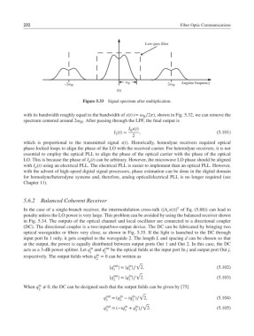
Figure 5.33 Signal spectrum after multiplication.
with its bandwidth roughly equal to the bandwidth of s(t) (= ∕2), shown in Fig. 5.32, we can remove the
B
spectrum centered around 2 . After passing through the LPF, the final output is
IF
I s(t)
0
I (t)= , (5.101)
2
2
which is proportional to the transmitted signal s(t). Historically, homodyne receivers required optical
phase-locked loops to align the phase of the LO with the received carrier. For heterodyne receivers, it is not
essential to employ the optical PLL to align the phase of the optical carrier with the phase of the optical
LO. This is because the phase of I (t) can be arbitrary. However, the microwave LO phase should be aligned
d
with I (t) using an electrical PLL. The electrical PLL is easier to implement than an optical PLL. However,
d
with the advent of high-speed digital signal processors, phase estimation can be done in the digital domain
for homodyne/heterodyne systems and, therefore, analog optical/electrical PLL is no longer required (see
Chapter 11).
5.6.2 Balanced Coherent Receiver
2
In the case of a single-branch receiver, the intermodulation cross-talk (|A s(t)| of Eq. (5.88)) can lead to
r
penalty unless the LO power is very large. This problem can be avoided by using the balanced receiver shown
in Fig. 5.34. The outputs of the optical channel and local oscillator are connected to a directional coupler
(DC). The directional coupler is a two-input/two-output device. The DC can be fabricated by bringing two
optical waveguides or fibers very close, as shown in Fig. 5.35. If the light is launched to the DC through
input port In 1 only, it gets coupled to the waveguide 2. The length L and spacing d can be chosen so that
at the output, the power is equally distributed between output ports Out 1 and Out 2. In this case, the DC
in
acts as a 3-dB power splitter. Let q and q out be the optical fields at the input port In j and output port Out j,
j j
in
respectively. The output fields when q = 0 can be written as
2
√
in
out
|q | = |q |∕ 2, (5.102)
1 1
√
in
out
|q | = |q |∕ 2. (5.103)
2 1
in
When q ≠ 0, the DC can be designed such that the output fields can be given by [75]
2
√
in
in
q out =(q − iq )∕ 2, (5.104)
1 1 2
√
in
in
q out =(−iq + q )∕ 2. (5.105)
2 1 2