
Page 381 - FUNDAMENTALS OF COMPUTER
P. 381
NPP
NPP CPU Architecture, Addressing Modes and Data Transfer Schemes 381
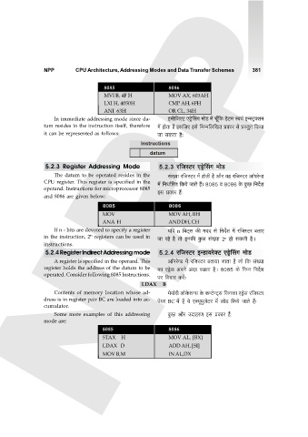
8085 8086
MVI B, 4F H MOV AX, 603AH
LXI H, 4050H CMP AH, 6FH
ANI 63H OR CL, 34H
In immediate addressing mode since da- B‘r{OEQ> ES´>oqgJ ‘moS> ‘| My±{H$ S>oQ>‘ ñd¶§ BÝñQ´>³eZ
tum resides in the instruction itself, therefore ‘| hmoVm h¡ Bg{bE Bgo {ZåZ{b{IV àH$ma go àñVwV {H$¶m
it can be represented as follows: Om gH$Vm h¡…
Instructions
datum
5.2.3 Register Addressing Mode 5.2.3 a{OñQ>a ES´>oqgJ _moS>
The datum to be operated resides in the g§»`m a{OñQ>a _| hmoVr h¡ Am¡a ¶h a{OñQ>a Am°naoÝS>
CPU register. This register is specified in the ‘| {ZYm©[aV {H$¶o OmVo h¢& 8085 d 8086 Ho$ Hw$N> {ZX}e
operand. Instructions for microprocessor 8085
and 8086 are given below: Bg àH$ma h¢:
MOV MOV AH, BH
ANA H AND DH, CH
If n - bits are devoted to specify a register `{X n {~Q>²g H$s _XX go {ZX}e _| a{OñQ>a ~VmE
n
in the instruction, 2 registers can be used in Om aho h¡ Vmo BZH$s Hw$c g§»`m 2 hmo gH$Vr h¡Ÿ&
n
instructions.
5.2.4 Register Indirect Addressing mode 5.2.4 a{OñQ>a BÝS>m`aoŠQ> ES´>oqgJ _moS>
A register is specified in the operand. This Am°naoÝS> _| a{OñQ>a ~Vm`m OmVm h¡ Omo {H$ g§»`m
register holds the address of the datum to be H$m ES´>og AnZo A§Xa aIVm h¡Ÿ& 8085 H$o {ZåZ {ZX}e
operated. Consider following 8085 Instructions.
na {dMma H$a|…
LDAX B
Contents of memory location whose ad- ‘o‘moar bmoHo$eÝg Ho$ H$ÝQ>oÝQ²>g {OZH$m ES´>og a{OñQ>a
dress is in register pair BC are loaded into ac- no¶a BC ‘| h¡ do E³¶y‘wboQ>a ‘| bmoS> {H$¶o OmVo h¢…
cumulator.
Some more examples of this addressing Hw$N> Am¡a CXmhaU Bg àH$ma h¡§:
mode are:
8085 8086
STAX H MOV AL, [BX]
LDAX D ADD AH, [SI]
MOV B,M IN AL,DX