
Page 183 - Handout of Computer Architecture (1)..
P. 183
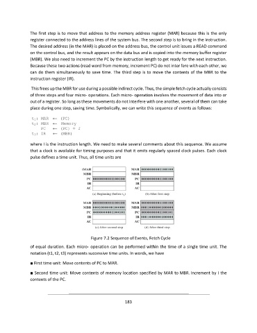
The first step is to move that address to the memory address register (MAR) because this is the only
               register connected to the address lines of the system bus. The second step is to bring in the instruction.
               The desired address (in the MAR) is placed on the address bus, the control unit issues a READ command
               on the control bus, and the result appears on the data bus and is copied into the memory buffer register
               (MBR). We also need to increment the PC by the instruction length to get ready for the next instruction.
               Because these two actions (read word from memory, increment PC) do not inter fere with each other, we
               can do them simultaneously to save time. The third step is to move the contents of the MBR to the
               instruction register (IR).

                This frees up the MBR for use during a possible indirect cycle. Thus, the simple fetch cycle actually consists
               of three steps and four micro- operations. Each micro- operation involves the movement of data into or
               out of a register. So long as these movements do not interfere with one another, several of them can take
               place during one step, saving time. Symbolically, we can write this sequence of events as follows:


               where I is the instruction length. We need to make several comments about this sequence. We assume
               that a clock is available for timing purposes and that it emits regularly spaced clock pulses. Each clock
               pulse defines a time unit. Thus, all time units are


                                            Figure 7.2 Sequence of Events, Fetch Cycle

               of equal duration. Each micro- operation can be performed within the time of a single time unit. The
               notation (t1, t2, t3) represents successive time units. In words, we have

               ■ First time unit: Move contents of PC to MAR.
               ■ Second time unit: Move contents of memory location specified by MAR to MBR. Increment by I the
               contents of the PC.


                                                             183