
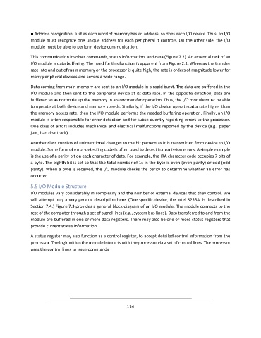
Page 114 - Handout of Computer Architecture (1)..
P. 114
■ Address recognition: Just as each word of memory has an address, so does each I/O device. Thus, an I/O
               module must recognize one unique address for each peripheral it controls. On the other side, the I/O
               module must be able to perform device communication.

               This communication involves commands, status information, and data (Figure 7.2). An essential task of an
               I/O module is data buffering. The need for this function is apparent from Figure 2.1. Whereas the transfer
               rate into and out of main memory or the processor is quite high, the rate is orders of magnitude lower for
               many peripheral devices and covers a wide range.

               Data coming from main memory are sent to an I/O module in a rapid burst. The data are buffered in the
               I/O module and then sent to the peripheral device at its data rate. In the opposite direction, data are
               buffered so as not to tie up the memory in a slow transfer operation. Thus, the I/O module must be able
               to operate at both device and memory speeds. Similarly, if the I/O device operates at a rate higher than
               the memory access rate, then the I/O module performs the needed buffering operation. Finally, an I/O
               module is often responsible for error detection and for subse quently reporting errors to the processor.
               One class of errors includes mechanical and electrical malfunctions reported by the device (e.g., paper
               jam, bad disk track).

               Another class consists of unintentional changes to the bit pattern as it is transmitted from device to I/O
               module. Some form of error-detecting code is often used to detect transmission errors. A simple example
               is the use of a parity bit on each character of data. For example, the IRA character code occupies 7 bits of
               a byte. The eighth bit is set so that the total number of 1s in the byte is even (even parity) or odd (odd
               parity). When a byte is received, the I/O module checks the parity to determine whether an error has
               occurred.

               5.5 I/O Module Structure
               I/O modules vary considerably in complexity and the number of external devices that they control. We
               will attempt only a very general description here. (One specific device, the Intel 8255A, is described in
               Section 7.4.) Figure 7.3 provides a general block diagram of an I/O module. The module connects to the
               rest of the computer through a set of signal lines (e.g., system bus lines). Data transferred to and from the
               module are buffered in one or more data registers. There may also be one or more status registers that
               provide current status information.
               A status register may also function as a control register, to accept detailed control information from the
               processor. The logic within the module interacts with the processor via a set of control lines. The processor
               uses the control lines to issue commands


                                                             114