


Page 98 - Handout Digital Electronics
P. 98
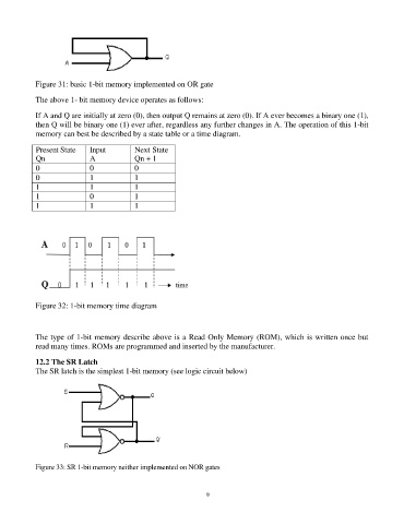
Figure 31: basic 1-bit memory implemented on OR gate

            The above 1- bit memory device operates as follows:

            If A and Q are initially at zero (0), then output Q remains at zero (0). If A ever becomes a binary one (1),
            then Q will be binary one (1) ever after, regardless any further changes in A. The operation of this 1-bit
            memory can best be described by a state table or a time diagram.

            Present State   Input         Next State
            Qn              A             Qn + 1
            0               0             0
            0               1             1
            1               1             1
            1               0             1
            1               1             1


            Figure 32: 1-bit memory time diagram


            The type of 1-bit memory describe above is a Read Only Memory (ROM), which is written once but
            read many times. ROMs are programmed and inserted by the manufacturer.


            12.2 The SR Latch
            The SR latch is the simplest 1-bit memory (see logic circuit below)


            Figure 33: SR 1-bit memory neither implemented on NOR gates


                                                                98

