
Page 190 - Fiber Optic Communications Fund
P. 190
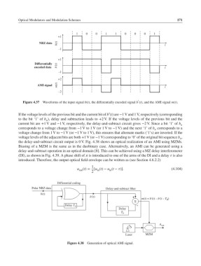
Optical Modulators and Modulation Schemes                                          171


                                         1    0    0    1    1    0     0    0    1
                               +1
                               b(t)                                                    t
                      NRZ data
                                –1

                               +1
                   Differentially
                   encoded data   b'(t)                                                t
                                –1

                               +2
                     AMI signal  m(t)                                                  t
                                –2

                                                                         ′
             Figure 4.37 Waveforms of the input signal b(t), the differentially encoded signal b (t), and the AMI signal m(t).

                                                          ′
           If the voltage levels of the previous bit and the current bit of b (t) are −1 V and 1 V, respectively (corresponding
           to the bit ‘1’ of b ), delay and subtraction leads to +2 V. If the voltage levels of the previous bit and the
                         n
           current bit are +1 V and −1 V, respectively, the delay-and-subtract circuit gives −2 V. Since a bit ‘1’ of b n
           corresponds to a voltage change from −1 V to 1 V (or 1 V to −1 V) and the next ‘1’ of b corresponds to a
                                                                                  n
           voltage change from 1 V to −1 V (or −1 V to 1 V), this ensures that alternate marks (‘1’s) are inverted. If the
           voltage levels of the adjacent bits are both +1 V (or −1 V) corresponding to ‘0’ of the original bit sequence b ,
                                                                                               n
           the delay-and-subtract circuit output is 0 V. Fig. 4.38 shows an optical realization of an AMI using MZMs.
           Biasing of a MZM is the same as in the duobinary case. Alternatively, an AMI can be generated using a
           delay-and-subtract operation in an optical domain [8]. This can be achieved using a MZ delay interferometer
           (DI), as shown in Fig. 4.39. A phase shift of  is introduced to one of the arms of the DI and a delay  is also
           introduced. Therefore, the output optical field envelope can be written as (see Section 4.6.2.2)
                                                 1
                                         u (t)=   [u (t)− u (t − )].                     (4.104)
                                          out       in    in
                                                 2

                               Differential coding
                  Polar NRZ data                         Delay-and-subtract filter
                      b(t)
                                                b'(t)                  +
                                                                           m(t) = b'(t) – b'(t – T B )
                                                                        Σ
                                                                         –
                                   Delay T b
                                                               Delay
                                                                T b


                                                                                     A out
                                                                   Laser     MZM

                                    Figure 4.38  Generation of optical AMI signal.