
Page 165 - GIGABYTE Service Manual-v3.0-110101
P. 165
04. Because contact area for the joint of thermal plane is bigger and is under the
MOSFET, visual inspection is not enough to confirm the reliability. In order to make
sure the wetting area in the contact area is enough, touch and press the MOSFET until it
can be moved smoothly on the PCB after solder has melted.
Caution: Any open of MOSFET soldering could cause M/B Burned out.
Figure 11-38: MOSFET Soldering-3
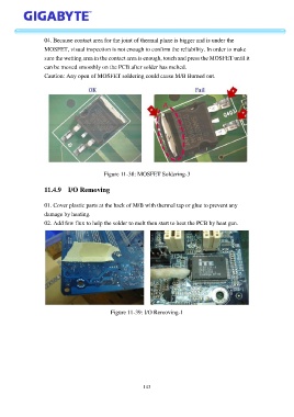
11.4.9 I/O Removing
01. Cover plastic parts at the back of M/B with thermal tap or glue to prevent any
damage by heating.
02. Add few flux to help the solder to melt then start to heat the PCB by heat gun.
Figure 11-39: I/O Removing-1
143