
Page 89 - GIGABYTE Service Manual-v3.0-110101
P. 89
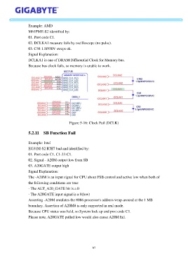
Example: AMD

                   M61PME-S2 identified by:
                   01. Post code C1.
                   02. DCLKA1 measure fails by oscilloscope (no pulse).
                   03. C58 1.5P/50V swaps ok.

                   Signal Explanation:
                   DCLKA1 is one of DRAM Differential Clock for Memory bus.
                   Because bus clock fails, so memory is unable to work.


                                             Figure 5-16: Clock Fail (DCLK)

                   5.2.11  SB Function Fail


                   Example: Intel
                   EG31M-S2 ICH7 bad and identified by:
                   01. Post code C1, C1-33-C1.
                   02. Signal - A20M output low from SB
                   03. A20GATE output high

                   Signal Explanation:
                   The -A20M is an input signal for CPU about FSB control and active low when both of
                   the following conditions are true:

                   - The ALT_A20_GATE bit is a 0
                   - The A20GATE input signal is a 0(low)
                   Asserting -A20M emulates the 8086 processor's address wrap-around at the 1 MB
                   boundary. Assertion of A20M# is only supported in real mode.
                   Because CPU status was held, so System lock up and post code C1.

                   Please note, A20GATE pulled low would also cause A20M fail.


                                                            67