
Page 238 - FUNDAMENTALS OF COMPUTER
P. 238
NPP
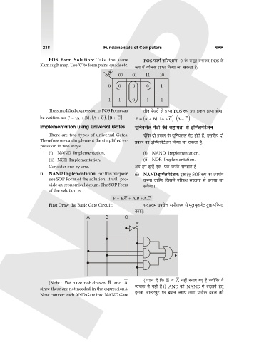
238 Fundamentals of Computers NPP
POS Form Solution: Take the same POS \$m_© gm°ë`yeZ: 0 Ho$ g_yh ~ZmH$a POS Ho$
Karnaugh map. Use ‘0’ to form pairs, quads etc. ê$n _| ì`§OH$ àmßV {H$`m Om gH$Vm h¡:
A B C 00 01 11 10
0 0 0 0 1
1 1 0 1 1
The simplified expression in POS Form can VrZ no`am| go àmßV POS ê$n Bg àH$ma àmßV hmoJm:
be written as: F = (A + B ) (A. + C ) (B. + C ) F = (A + B ) (A. + C ) (B. + C )
Implementation using Universal Gates `y{Zdg©b JoQ>m| H$s ghm`Vm go Bpåßb_|Q>oeZ
There are two types of universal Gates. My±{H$ Xmo àH$ma Ho$ `y{Zdg©b JoQ> hmoVo h¢, Bg{bE Xmo
Therefore we can implement the simplified ex- àH$ma H$m Bpåßb_|Q>oeZ {H$`m Om gH$Vm h¡:
pression in two ways:
(i) NAND Implementation. (i) NAND Implementation.
(ii) NOR Implementation. (ii) NOR Implementation.
Consider one by one. A~ h_ BÝh| EH$-EH$ H$aHo$ g_PVo h¢Ÿ&
(i) NAND Implementation: For this purpose (i) NAND Bpåßb_|Q>oeZ: Bg hoVw SOP ê$n H$m Cn`moJ
use SOP Form of the solution. It will pro- H$aZm Mm{hE {Oggo n[anW gabVm go ~Zm¶m Om
vide an economical design. The SOP Form gHo$JmŸ&
of the solution is
F = C . B + B . A + C . A
First Draw the Basic Gate Circuit: gd©àW_ Cnamoº$ g_rH$aU go _yb^yV JoQ> `wº$ n[anW
~ZmE:
A B C
C
F
(Note : We have not drawn B and A (Ü`mZ X| {H$ B d A Zht ~ZmE JE h¢ Š`m|{H$ do
since these are not needed in the expression.). ì`§OH$ _| Zht h¢Ÿ&) AND H$mo NAND _| ~XbZo hoVw
Now convert each AND Gate into NAND Gate BgHo$ AmCQ>nwQ> na ~~b bJmE VWm àË`oH$ ~~b H$mo