
Page 410 - Maxwell House
P. 410
390 Chapter 8
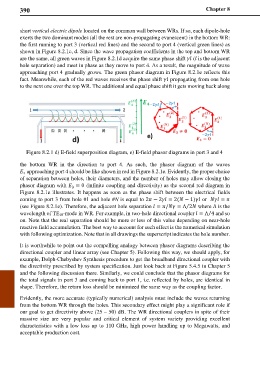
short vertical electric dipole located on the common wall between WRs. If so, each dipole-hole
exerts the two dominant modes (all the rest are non-propagating evanescent) in the bottom WR:
the first running to port 3 (vertical red lines) and the second to port 4 (vertical green lines) as
shown in Figure 8.2.1c, d. Since the wave propagation coefficients in the top and bottom WR
are the same, all green waves in Figure 8.2.1d acquire the same phase shift ( is the adjacent
hole separation) and meet in phase as they move to port 4. As a result, the magnitude of wave
approaching port 4 gradually grows. The green phasor diagram in Figure 8.2.1e reflects this
fact. Meanwhile, each of the red waves receives the phase shift propagating from one hole
to the next one over the top WR. The additional and equal phase shift it gets moving back along
e)
Figure 8.2.1 d) E-field superposition diagram, e) E-field phasor diagrams in port 3 and 4
the bottom WR in the direction to port 4. As such, the phasor diagram of the waves
approaching port 4 should be like shown in red in Figure 8.2.1e. Evidently, the proper choice
4
of separation between holes, their diameters, and the number of holes may allow closing the
phasor diagram with = 0 (infinite coupling and directivity) as the second red diagram in
3
Figure 8.2.1e illustrates. It happens as soon as the phase shift between the electrical fields
coming to port 3 from hole #1 and hole #N is equal to 2 − 2 = 2( − 1) or =
(see Figure 8.2.1e). Therefore, the adjacent hole separation = / = Λ 2 where Λ is the
⁄
wavelength of TE10-mode in WR. For example, in two-hole directional coupler = Λ 4 and so
⁄
on. Note that the real separation should be more or less of this value depending on near-hole
reactive field accumulation. The best way to account for such effect is the numerical simulation
with following optimization. Note that in all drawings the superscript indicates the hole number.
It is worthwhile to point out the compelling analogy between phasor diagrams describing the
directional coupler and linear array (see Chapter 5). Following this way, we should apply, for
example, Dolph-Chebyshev Synthesis procedure to get the broadband directional coupler with
the directivity prescribed by system specification. Just look back at Figure 5.4.5 in Chapter 5
and the following discussion there. Similarly, we could conclude that the phasor diagrams for
the total signals in port 3 and coming back to port 1, i.e. reflected by holes, are identical in
shape. Therefore, the return loss should be minimized the same way as the coupling factor.
Evidently, the more accurate (typically numerical) analysis must include the waves returning
from the bottom WR through the holes. This secondary effect might play a significant role if
our goal to get directivity above (25 – 50) dB. The WR directional couplers in spite of their
massive size are very popular and critical element of system variety providing excellent
characteristics with a low loss up to 110 GHz, high power handling up to Megawatts, and
acceptable production cost.